| Duration: | 04/2020 - 12/2024 |
| Contracting Authority/ Sponsors: |
Federal Ministry of Economic Affairs and Climate Action (BMWK) Fkz: 03EE1046A |
| Project Partners: | Fraunhofer ISE; AZUR SPACE Solar Power GmbH; DISCO Hi-Tec Europe GmbH; SiLi Technologies GmbH; Fuchs Design GmbH; Fela GmbH; Wagenbrett GmbH & Co. KG; Technische Universität Berlin |
| Project Focus: |
micro-CPV – Development of a Highly Concentrating CPV Module Based on Modern Micro-Production Technology


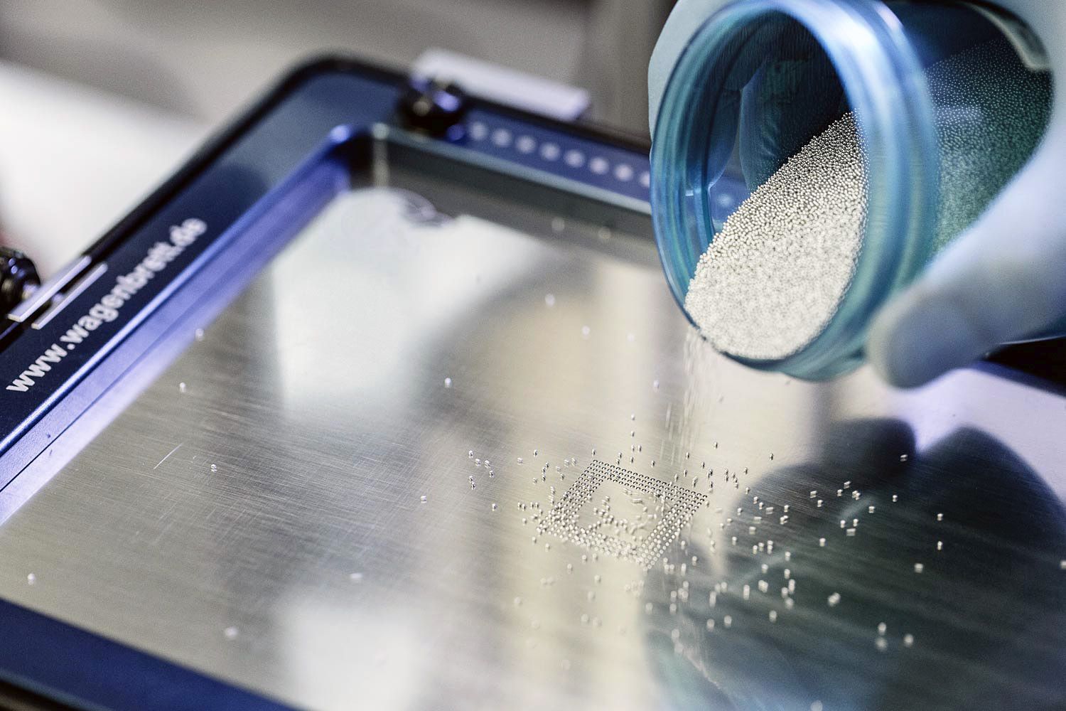
Innovative manufacturing technologies, e.g. for large-area displays, enable the cost-effective production of units consisting of thousands of interconnected semiconductor devices by miniaturization, additive manufacturing, parallelization and self-alignment. The objective of the "micro-CPV" joint project was to develop a concentrator photovoltaic (CPV) module based on these technologies, which enables high PV performance while at the same time exploits cost reduction potentials in production.
Concentrating photovoltaics (CPV) achieves the highest efficiency and lowest energy payback times of all photovoltaic technologies. The up to 1000-fold optical concentration increases the efficiency and reduces the solar cell area used. This means that more expensive but highly efficient III-V multi-junction solar cells can be used for terrestrial applications. In 2022, Fraunhofer ISE set a new record for the conversion of solar radiation into electrical power with an efficiency of 47.6% using a concentrator solar cell. The industrial implementation of CPV technology has already been demonstrated in numerous multi-MW power plant installations. However, module costs need to be reduced further in order to remain competitive. This is where the joint project "micro-CPV" comes in, in which synergies with products from microelectronics, optoelectronics and display production were evaluated for a significant cost reduction of highly efficient CPV modules. Rapid progress in the areas of miniaturization, additive manufacturing, parallelization and self-alignment, driven among other things by the development of displays based on µ-LEDs, promises a steep learning curve and cost degression.
In this project, we developed a micro-CPV module with a low-cost lens array that focuses the light onto a spherical lens secondary optic and then onto the miniature III-V concentrator solar cell. This configuration allows both 1000-fold sunlight concentration and a high acceptance angle for module alignment with a flat design of a few centimeters.
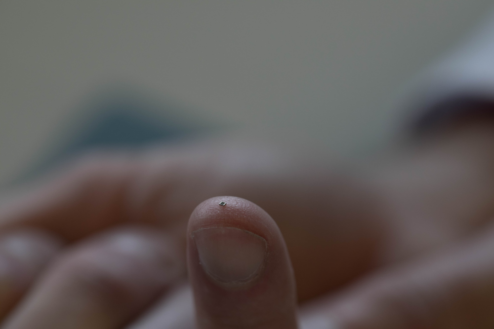
Advanced additive circuit board technologies in combination with panel-level packaging processes were applied for the base plate. Micro-concentrator solar cells with an area of just a fraction of a square millimeter are separated with minimized kerf loss and then mounted and interconnected directly onto the panel in a self-aligning manner. Because the solar cells are so small, the cell operating temperature remains acceptable in spite of the exposure to high sun concentrations and the absence of a dedicated heat sink.
The high innovation potential in this research and development project was the result of the outstanding technological expertise of the various partners involved, who covered the CPV value chain from individual components and processes through to finished modules.
Initially, small test modules with 3×3 interconnected solar cells were produced in the project and used to evaluate the various technology components, such as solar cell structures, circuit board designs, spherical lenses and primary lens plates. Technological aspects and the impact on module performance as well as economic aspects were taken into account for the evaluation.
As a next step a demonstrator module was developed, which consists of an array of 6×10 cell-lens units with an aperture area of 205 cm². This demonstrator module has been undergoing field testing since 2023. A filtered performance evaluation carried out according to IEC 62670-3 criteria shows a CSTC (concentrator standard test conditions) efficiency of 36% (see graph, or the full scientific paper here).
In addition to the development of new components and manufacturing technologies, another focus of the project was on model-based understanding of the interrelationships within the module. By employing a novel nested optical-electrical Monte Carlo modeling approach, we quantitatively analyzed the impact of various tolerances, i.e. slight deviations in the size and arrangement of components that occur in real modules, on overall performance. The insights gained from this analysis are instrumental in guiding further development efforts, highlighting areas where enhancements can yield the most significant benefits, as well as identifying opportunities where slightly relaxed tolerances can provide techno-economic advantages.
Components and manufacturing processes as well as packaging technologies were transferred to larger modules in the 24"×18" panel format (>2000 cm²), a standard format in PCB industry and from panel-level packaging in microelectronics. Outdoor measurements of a first panel-format micro-CPV module are in progress and results are expected soon.
To exploit the research and development results of this project, we are currently preparing a spin-off company to commercialize this promising technology. If you are interested, please contact Dr. Frank Dimroth.
More Information on this Topic:
- Cost Competitive Tracker Prototype for Next generation Concentrating Photovoltaics
- Fraunhofer ISE Develops the World's Most Efficient Solar Cell with 47.6 Percent Efficiency
- Power Rating of a Novel Micro-CPV Module Concept and Operational Influences (IEEE Journal of Photovoltaics)
- Effect of manufacturing tolerances on Micro-CPV assemblies: A quantitative approach based on statistical modeling (Solar Energy Materials and Solar Cells)
- Two-step nested optical-electrical Monte-Carlo approach to analyze the influence of tolerances on Micro-CPV module performance (Solar Energy Materials and Solar Cells)
- Young Scientist Award auf der CPV-18 Konferenz
- Forced Motion Activated Self-Alignment of Micro-CPV Solar Cells (IEEE Journal of Photovoltaics)
- Technical boundaries of micro-CPV module components: How small is enough? (Proceedings of the 17th International Conference on Concentrator Photovoltaic Systems (CPV-17)


