High-Throughput Laser Processing

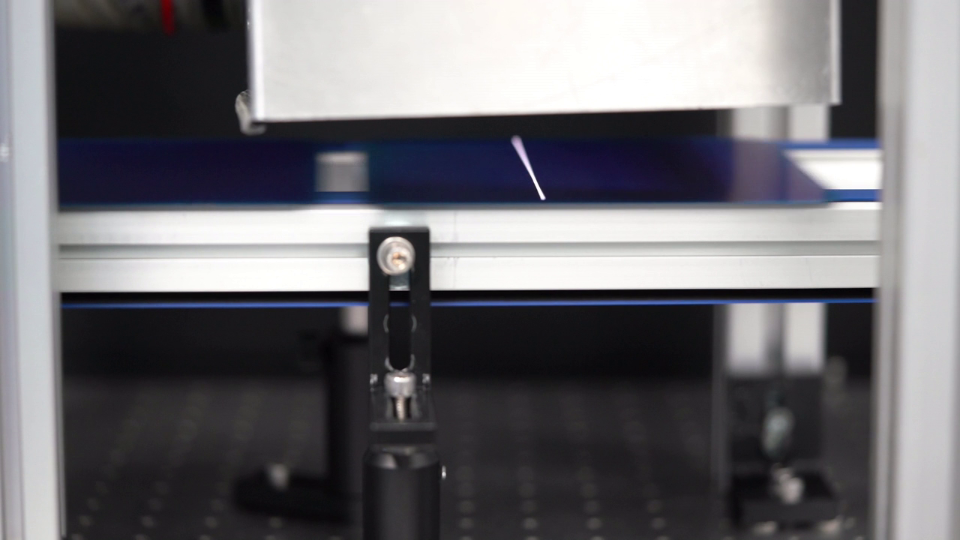
Photo of on-the-fly laser processing of solar cells.
© Fraunhofer ISE
Photo of on-the-fly laser processing of solar cells.

Galvanometer scanners, which can move the beam at up to 50 m/s over the sample by means of two mirrors, are usually used for fast beam alignment in laser material processing of silicon solar cells. Significantly higher processing speeds can be achieved with polygon scanners. Here, the laser beam hits a rotating polygon wheel consisting of several facets. The laser beam is then reflected from the facet onto the sample. Using a galvanometer mirror, the laser beam is also deflected transversely to this fast axis so that two-dimensional structures can be processed. Due to the high rotational speed of the polygon wheel, speeds of more than 1 km/s can be achieved, depending on the imaging optics.

Linear or rotary table systems are often used to transport the silicon wafer to the processing position. With both of these system concepts, the wafer is halted after it has been moved to the processing position and then laser processing is performed. With on-the-fly processing, however, the wafer lies on a conveyor belt and is processed as it passes underneath the laser scanner. This allows for a higher throughput, since there is no need to stop the conveyor belt and the distance between the individual wafers can be minimized.

Special optical sensor technology detects the position of the workpiece, enabling the laser process to be triggered at the right time.
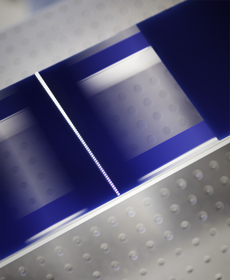
Polygon scanner
© Fraunhofer ISE
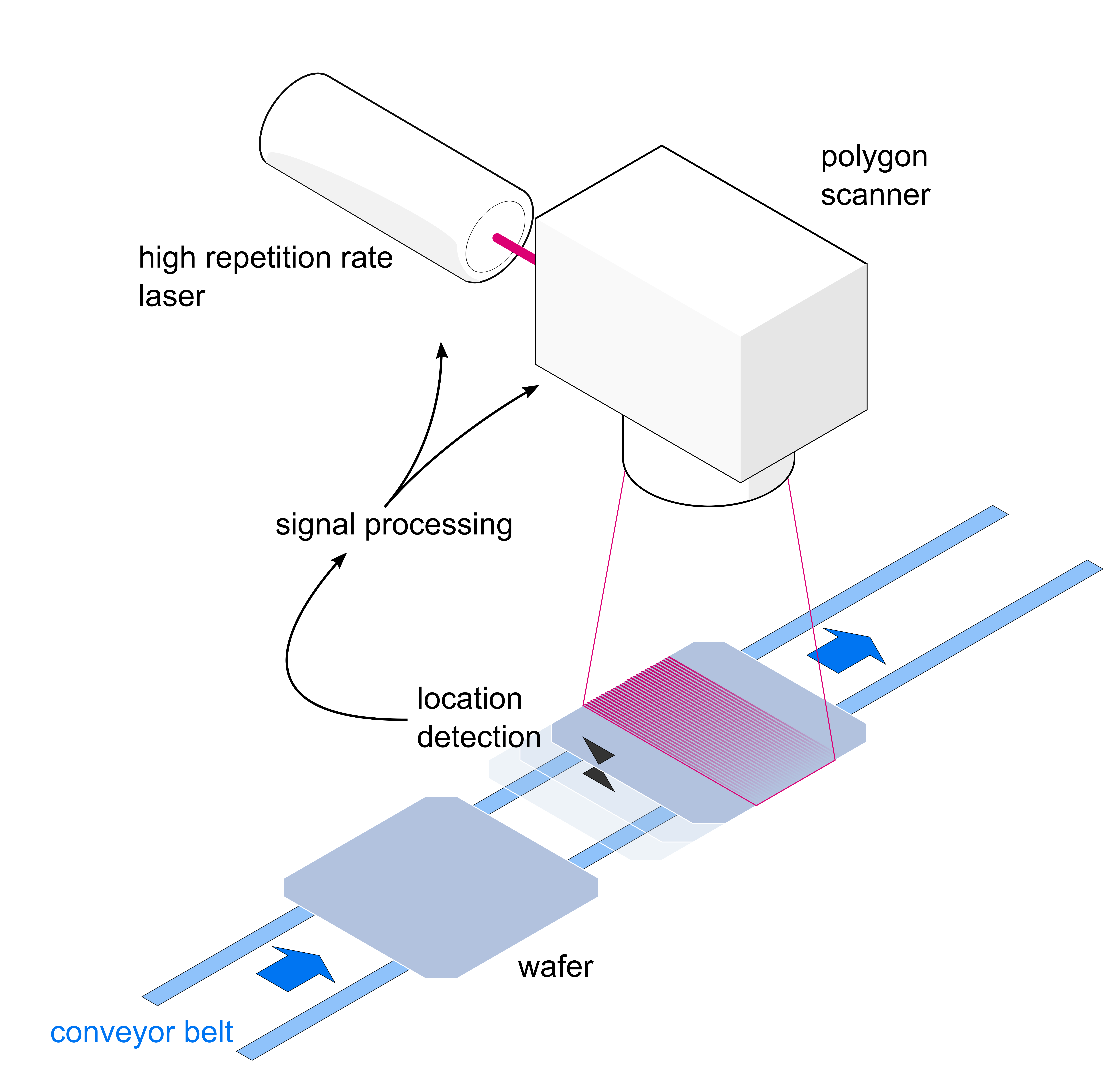
Schematic representation of on-the-fly processing with a polygon scanner. The workpiece is transported on a conveyor belt underneath the scanner. Its position is detected by optical sensors and signals are generated for the laser and the scanner.

The laser system construction team developed sensors and a setup to demonstrate this approach. The process of laser contact opening of the passivated back side of a PERC solar cell was performed at a high speed. The fast axis of the polygon is transverse to the direction of the belt. The pulse spacing results from the repetition rate of the laser and the polygon speed. Along the conveyor belt, the line spacing results from the speed of the belt and the jump speed of the Galvo mirror. The wafer is transported with a belt speed of up to 900 mm/s. Since the distance between two wafers on the belt can also be very small, a throughput of more than 15,000 wafers/h can be achieved.

Our service offer:

  • Implementation of on-the-fly polygon scan technology
  • Optimization of the processing strategy
  • Implementation of other optics and scanners
  • Integration of optical position sensors

Video: High-Throughput On-the-Fly Laser Processing

Privacy warning

With the click on the play button an external video from www.youtube.com is loaded and started. Your data is possible transferred and stored to third party. Do not start the video if you disagree. Find more about the youtube privacy statement under the following link: https://policies.google.com/privacy

Language: English | Duration: 0:56 Min.

Our on-the-fly laser processing technology enables a throughput of up to 15000 silicon wafer-based solar cells per hour per scanner. We have developed a combination of smart sensors and polygon-based laser scanning at deflection velocities of up to 1000m/s to achieve almost an order of magnitude increase in productivity compared to conventional systems.

The process seen in this video is known as “laser contact opening.” It is applied to the majority of solar cells produced today.