At the "Center for Functional Surfaces", we develop functional surfaces for a wide range of applications. We use large-area coating and structuring processes for this purpose.
Withe the coating technology, we develop solutions based on the sputtering process for the areas of photovoltaics, solar thermal energy, buildings, thin-film batteries and hydrogen technology. Applications include transparent electrodes and colored cover glass (MorphoColor®) for photovoltaics, low-emissivity and solar control coatings, optically switchable systems, bird protection glass and radio-transparent insulating glass as well as vacuum insulation glazing for energy-efficient buildings, protective coatings for fuel cells and electrolysers or absorber and mirror coatings in the field of solar thermal energy and concentrating solar thermal power plants. Our coatings increase the energy efficiency of buildings, replace expensive materials, increase efficiency, extend service life or make the use of PV on facades attractive.
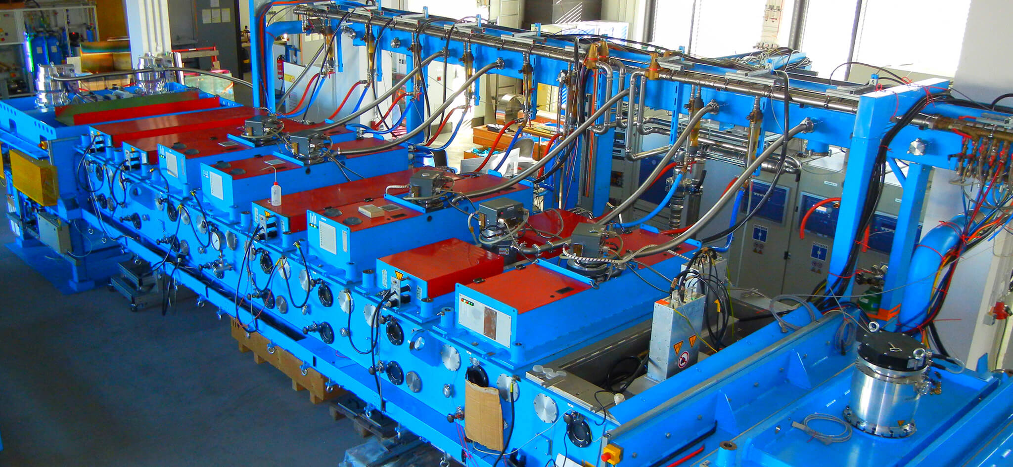
We can coat pilot series and demonstrators up to a size of 6m x 1.5m on our largest sputtering system with 9 planar and double-tube cathodes as well as a plasma etching station and PECVD source. In addition to optimizing the functional properties, we develop the coating systems for the respective requirements of the end product, e.g. long-term stability in outdoor use and industrial scalability. We also offer support with the system integration of the functional coating systems, e.g. in the module or in the façade.
Our range of services includes feasibility studies, small series production and product development through to finished industrial prototypes.
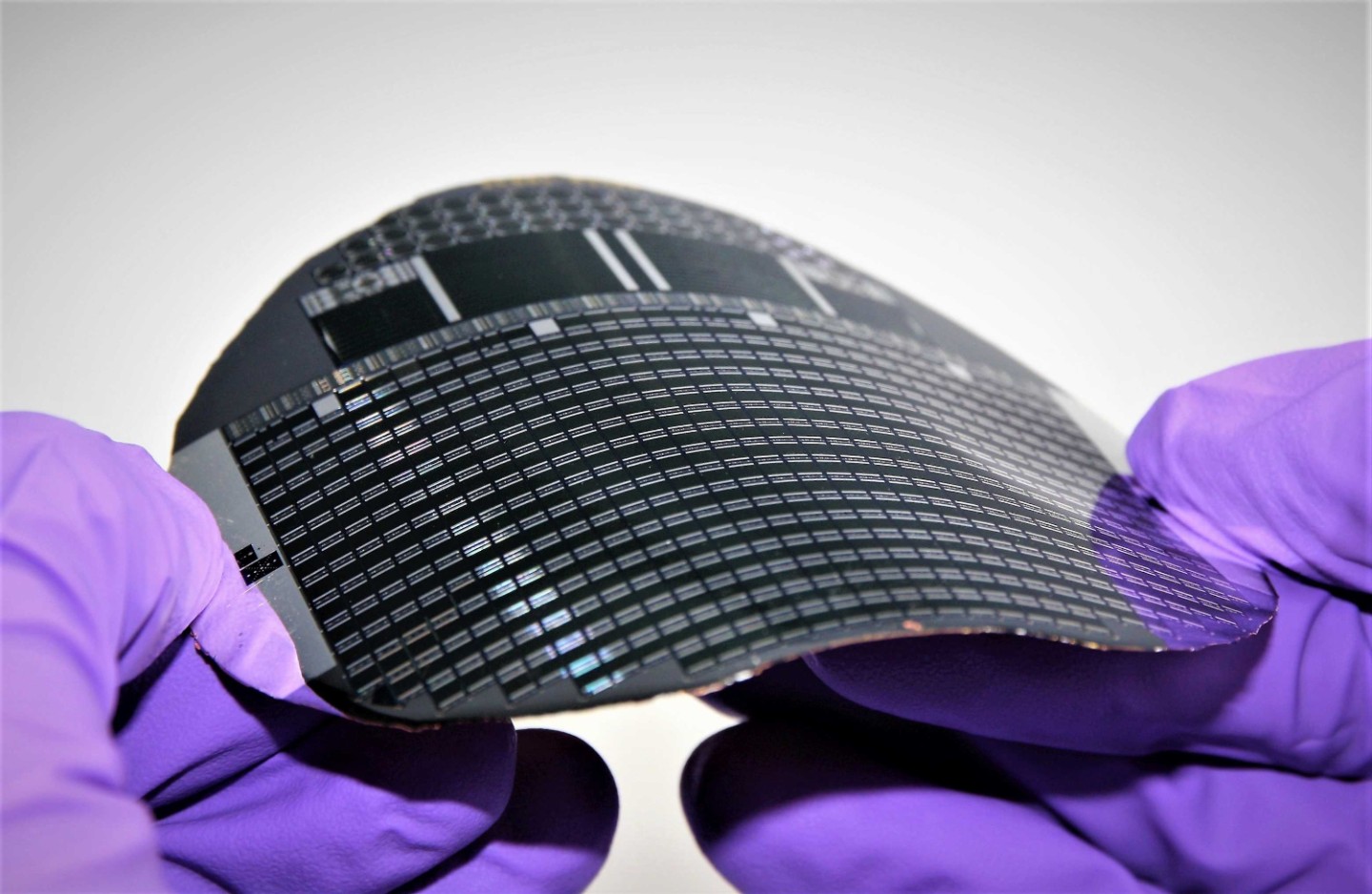
The structuring of surfaces in the micro- and nanometer range enables a breadth of optical and non-optical functionalities. The basis for the industrial feasibility of such surface structures is usually the large-scale production in customized shapes and dimensions. In solar cells, photonic nanostructures can be used to enhance absorption of sunlight and "capture" photons. In lighting applications, micro- and nanostructures enable light to be specifically extracted from LEDs, for example, and directed in the desired direction. In displays, functional structures are used for anti-reflective coating, polarization-optical applications or light guidance. Micro- and nanostructures also play a role in the modification of non-optical properties, e.g. in influencing the wettability, adhesion or friction of surfaces.
Technical Equipment
Vacuum Coating Technology Center Horizontal inline sputtering system (HIP)Coating area of up to 1.5m x 6m; chamber height of 16cm9 planar and double tube cathodesPECVD sourcePlasma etching stationCoating of curved substrates and tubesSubstrate types: Glass panes, polymer films and metal sheetsVertical inline sputtering system (VIP)Coating area of up to 1.1m x 0.65m; chamber height: 4cm5 planar and double tube cathodesPlasma etching stationLaboratory-scale sputtering systemCoating substrates of approx. 150mm diameter3 planar cathodes with 1 RF and 2 DC sourcesCo-sputtering possibleDoctor-blade system for homogeneous application of lacquers, DIN A4
Nanoimprint systems for transferring micro- and nanostructures to prototypesRoller nanoimprint setup for production-related processesPlasma etching systems with a variety of etching gases for transferring imprinted structures to non-polymeric materialsVapor deposition systems for coating metallic and dielectric layer systemsWave-optical modeling of complex photonic structures
Lab Characterization of Functional Surfaces Fourier spectrometer for optical characterizationScanning electron microscope (SEM)Atomic force microscope (AFM)White light interference microscopeEnergy dispersive X-ray spectroscopy (EDX)X-ray fluorescence analysis (XRF)Light microscopeMeasurement of layer stresses in thin layersMechanical abrasion testsElectrochemical characterization methodsVarious ovens of different sizes for different environmental conditions (air, vacuum, gases)Two climate chambers for weathering tests |


