Galvanic Metallization for Solar Cells

The metallization of solar cells is one of the largest cost factors in the manufacturing process. It has a significant influence on both cell efficiency and module connection.  

While silver is still the main contact material used in production, we at Fraunhofer ISE have been developing alternative manufacturing processes based on copper for many years. This saves costs, achieves the same solar cell efficiencies and ensures the availability of the required materials even in the rapidly growing photovoltaic market.  

We develop galvanic metallization processes for various types of solar cells. Laser structuring of the anti-reflective layer is used for both TOPCon and PERC solar cells, and a layer stack of nickel, copper and an ultra-thin silver finish is then deposited from the chemical solution.  

For silicon heterojunction and perovskite solar cells, special measures are required to avoid deposition over the entire surface of the transparent, conductive oxide. At the same time, sensitive functional layers must be protected from corrosion by the galvanic baths. We have developed innovative solutions to realize galvanic copper contacts for these challenging applications as well.  

Even on III-V or germanium materials, galvanic metal processes are interesting alternatives for highly conductive and cost-efficient contacts. Even though material costs usually play a less important role here, galvanic metal deposition also allows for very high-performance metal contacts under economic conditions.  . 

Galvanic Metallization of TOPCon Solar Cells

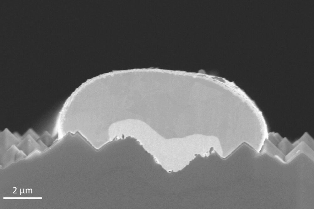
Elektronenmikroskopische Aufnahme eines Nickel-Kupferkontaktes mit hauchdünnem Silbercapping auf einer TOPCon-Solarzelle.
© Fraunhofer ISE
Electron micrograph image of a nickel-copper contact with wafer-thin silver capping on a TOPCon solar cell.

We work with you to develop galvanic deposition processes on your silicon substrate.

From plant engineering to the selection of suitable electrolytes to structuring and process control, we are your partner for electrochemical metal deposition on silicon.  

Of course, our main focus is on deposition for solar cells. In addition to our electroplating expertise and an extensive partner network, we also offer a complete characterization of all cell and metallization properties. We also have a comprehensive range of equipment in this area, from a laboratory system for processing individual wafers to an industry-ready production system with a throughput of several hundred wafers per day. This applies to both the electroplating processes and laser structuring.  

We are in contact with many different partners in the fields of plant engineering, materials development and process integration. If necessary, we have the expertise to develop our own solutions.

Galvanic Metallization of III-V Semiconductors

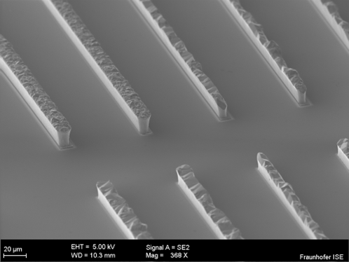
Galvanisch erzeugte Silberkontakte mit sehr hoher Leitfähigkeit auf einer III-V Solarzelle zur Übertragung hoher elektrischer Leistungen bis 35W/cm² mit Laserstrahlung.
© Fraunhofer ISE
Galvanically generated silver contacts with very high conductivity on a III-V solar cell for the transmission of high electrical power up to 35W/cm² with laser radiation.

We develop solutions for the deposition of the typical galvanically depositable metals and metal layer stacks on a wide variety of semiconductor materials.  

We have extensive experience in the coating of III-V semiconductors (GaAs, GaInP, etc.) as well as in the coating of germanium. In addition to the coating itself, we also provide solutions for structuring, as well as pre- and post-conditioning.  

For other materials, we draw on a wealth of experience and an extensive pool of equipment to achieve the desired process result.