Lab Structuring and Photonics

We develop solutions based on micro- and nanostructures for solar cells and other photovoltaic components such as photovoltaic cells for transmitting power using laser light, but also for related components such as LEDs. The technical focus is on a combination of nanoimprint lithography with different structures, photolithography, physical vapor deposition processes and wet and dry chemical etching processes.

Our range of services includes feasibility studies, small series production and product development up to finished industrial prototypes. We cover the entire spectrum from photonic design and process development to the characterization of prototypes and small series.

As we are experts in both nanostructuring and the realization of highly efficient solar cells, we can use nanostructures profitably in solar cells without impairing them electrically. We can map the entire process chain from the wafer to the photonic component.

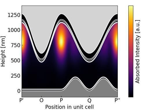
Wave Optical Modeling / Design of Photonic Structures for Use in Photolvoltaic Cells and LEDs.

Ergebnisse der wellenoptischen Modellierung einer strukturierten Perowskitsolarzelle.
© Fraunhofer ISE
Wave optical modeling results of a structured perovskite solar cell.

Using RCWA, we design and optimize structures for improved light coupling in and out, for light tapping or for coupling in resonant modes. We also measure and evaluate manufactured structures by means of reflection and transmission measurements or on solar cell structures in order to determine their effect on the relevant measured variables of solar cells. We are able to take the specifics of PV components (e.g. necessary contact fingers) into account at the design stage.

Process Development of Nanostructuring of LEDs and PV Components

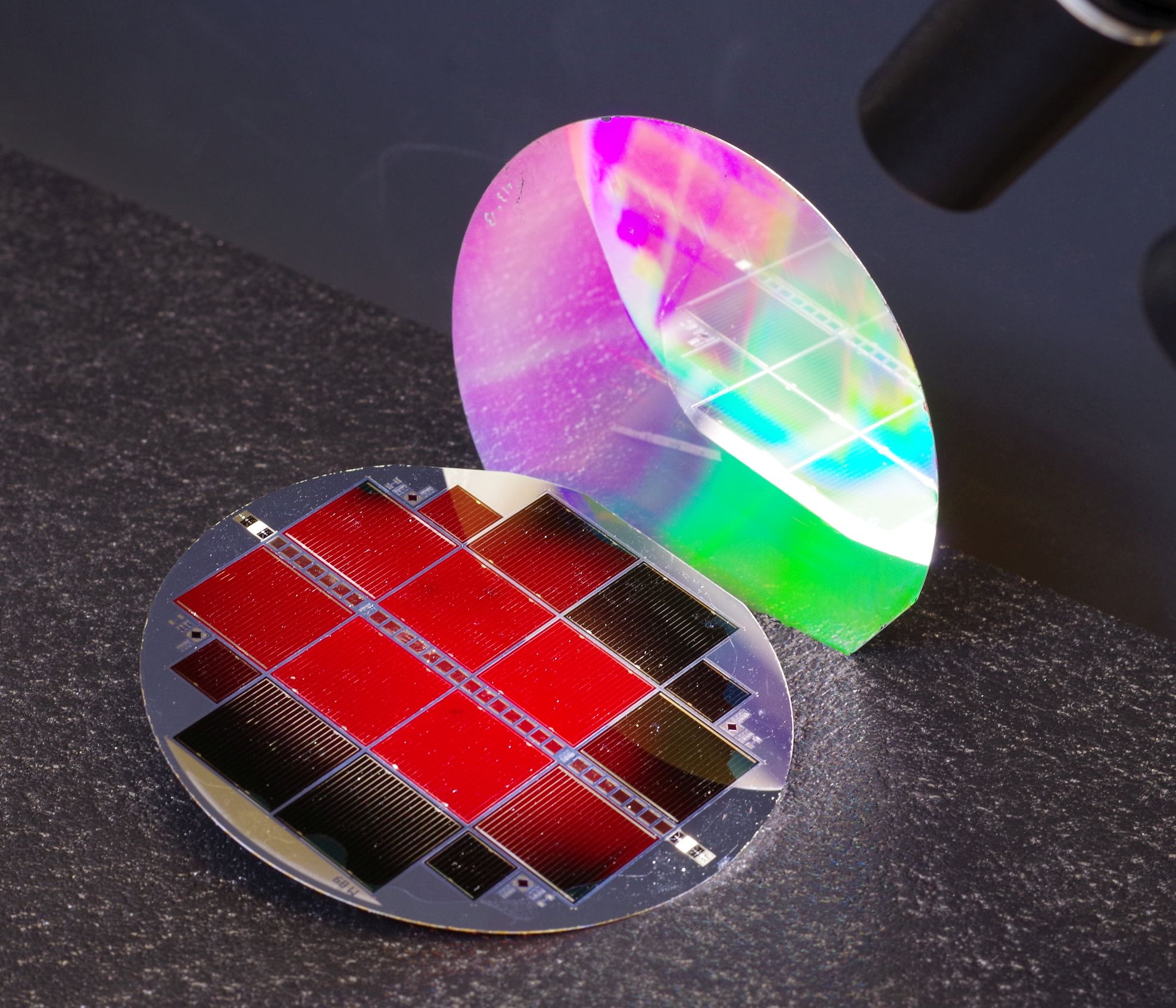
III-V // silicon tandem solar cell with 35.9 % efficiency.
© Fraunhofer ISE
The new III-V // silicon tandem solar cell with 35.9 % efficiency. The top subcells, made of GaInP, glow red under illumination. This is a sign of outstanding material quality. The back side of the cell shimmers in rainbow colors, because a nanostructure was used on this side to increase the efficiency.

We develop and optimize nanoimprint and etching processes for implementing photonic structures in electrically active components, primarily for PV components and LEDs, but also for other applications. We can map the entire process chain and evaluate the function of photonic structures in the final component. To do this, we combine various processes - photolithography processes, vapor deposition of metals and dielectric layers, wet and dry chemical etching processes, electroplating and others - with nanoimprint lithography steps, enabling us to integrate nanostructures into complex components. We can imprint structures with element sizes from a few 100 nm to over 100 µm on up to 6” wafers.

Characterization (of Photonic Nanostructures)

Probe in einem Rasterkraftmikroskop.
© Fraunhofer ISE
Sample in an atomic force mircoscope.

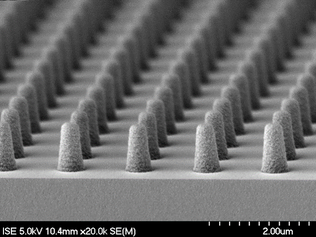
In close coordination with our customers, we evaluate the realized nanostructures using scanning electron microscopy (SEM), atomic force microscopy (AFM), spectrometry and electrical measurements in the final component. On the one hand, we examine the quality of the nanostructures, on the other hand, we evaluate their function in the finished component and can use this as a basis to optimize process chains or compare and optimize different nanostructures with regard to their function in the final component.