Laser Structuring of High-Precision Printing Forms

The metallization of silicon solar cells with ultra-fine contacts is one of the most demanding disciplines of functional screen printing . Decades of development of high-precision fine-mesh screens and rheologically specialized metal particle pastes now enable the printing of high-quality conductive contacts with a width of <10 µm. An essential factor for the process are the high-precision structured fine-mesh screens based on a stainless steel mesh. This mesh consists of up to 200 wires per centimeter or 520 wires per inch with wire thicknesses that are five  to ten times thinner than a human hair. To create a functional printing screen, the mesh is coated with a flexible top layer that is selectively opened in the printing sections using UV exposure or laser ablation.

Together with project partners, Fraunhofer ISE has developed a new platform based on ultrashort pulse laser technology and high-precision 3D scanning technology in the “Laser2Screen” project. This innovative laser solution enables the structuring of fine-mesh screens and metal foil stencils with previously unattainable precision of up to <2 µm. What is particularly revolutionary is that the fully digital laser process replaces conventional photolithography methods and offers flexible adaptation to workpiece variations as well as integrated optical measurement of the generated structures – all in a single device.  

This sustainable laser technology, which does not require chemical etchants or photoresists, not only enables new possibilities for solar cell metallization, but also screen and stencil structuring for demanding applications in opto-electronics, semiconductor manufacturing, and packaging technology.

Laser Structuring of Fine Mesh Screens

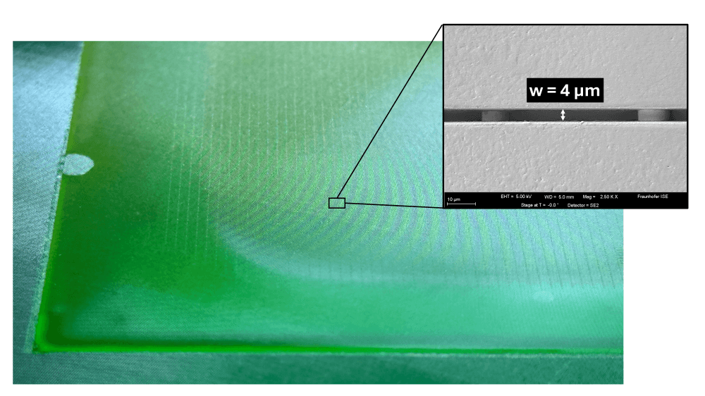
Laserstrukturiertes Feingewebe-Sieb mit Rasterelektronenmikroskop-  Detailaufnahme eines Siebkanals.
© Fraunhofer ISE
Laser-structured fine mesh screen with scanning electron microscope detailed image of a screen channel.

The precise laser technology of Fraunhofer ISE enables the highly accurate structuring of fine-mesh screens for the most demanding printing processes. Our ultrashort laser pulses remove the top layer of the screen with the utmost precision, resulting in sharp contours and perfectly defined openings. 

Our laser technology is particularly impressive when used with mesh-based screens, which can have up to 200 wires per centimeter and wire thicknesses five to ten times thinner than a human hair. Laser-based screen fabrication enables printing structures for photovoltaics that cannot be realized using conventional methods. The digital laser process also offers the possibility to customize the screen structuring to each individual mesh, taking even the smallest irregularities in the wire mesh into account.

Thanks to our close cooperation with leading mesh manufacturers, we are able to equip R&D partners with state-of-the-art screens. The subsequent in-house printing evaluation ensures that the fabricated screens meet the highest quality standards.

Laser Structuring of Metal Foil Stencils

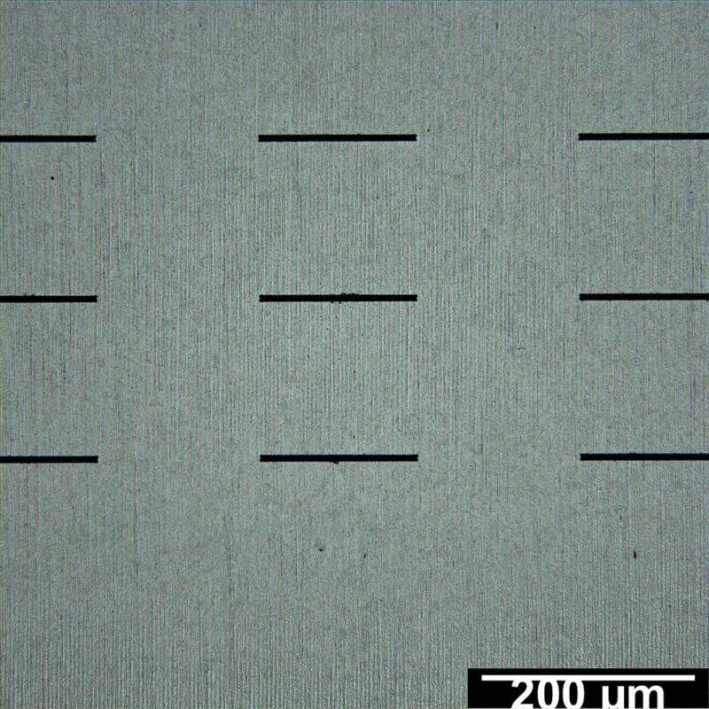
Präzise laserstrukturierte Öffnungen in einer Metallfolien-Schablone.
© Fraunhofer ISE / Foto: Andreas Brand
Precisely laser-structured openings in a metal foil stencil.

Stencil printing using metal foil stencils has been an established process in the electronics manufacturing section for decades, for example, to realize solder pastes, solder resists or conductive structures using printing technology. With our ultrashort pulse laser technology, we structure metal foil stencils with previously unattainable precision. In contrast to woven, mesh-based screens, these stencils consist of a thin, homogeneous metal foil, which can be structured using the laser process with finest openings of up to 2 µm in width and with almost vertical channel walls.  

These precision stencils open up completely new fields of application in semiconductor and electronics manufacturing. Typical applications include the application of solder pastes, conductive adhesives or functional materials for microelectronics. In this section, precisely defined layer thicknesses and exact edge geometries are crucial.

The digital laser process enables flexible adaptation to individual requirements and can realize even the most complex structures. Compared to conventional etching processes, laser structuring not only offers ecological advantages by eliminating the use of chemicals, but also higher precision and better reproducibility. 

We develop and manufacture specialized metal foil stencils for your specific R&D applications and support you in process optimization.

Evaluation of Screens and Stencils

Using Precision Screen Printing Equipment at the PVTEC of the Fraunhofer ISE

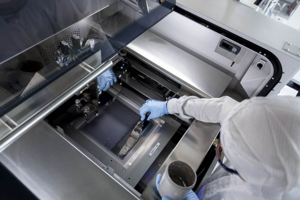
Siebdruck-Metallisierungsprozess am Fraunhofer ISE.
© Fraunhofer ISE / Foto: Dirk Mahler
Precision screen printing using metal pastes in Fraunhofer ISE PVTEC.

Technical screen printing with functional pastes requires special machinery and precise processes to ensure printing results of the highest quality and reproducibility. Fraunhofer ISE has decades of experience in the section of precision screen printing for photovoltaics and electronic applications. A central aspect of this work is the close collaboration with manufacturers of precision screens, stencils and pastes to identify the best possible material combination for a specific application. Fraunhofer ISE supports you in the design, evaluation and analysis of precision screen printing processes for all applications in the field of photovoltaics, electronics and other applications in the field of technical screen printing.

Microscopic and Electrical Analysis of Screen/Stencil Structuring and Printing Results

Using Highly Automated Image Analysis Methods

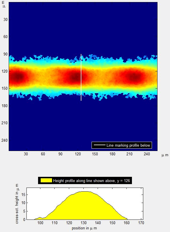
Automatisierte Analyse und statistische Auswertung der Druckergebnisse mithilfe von Bildanalyse-Verfahren.
© Fraunhofer ISE
Automated analysis and statistical evaluation of the print results using image analysis methods.

The analysis and evaluation of print results for technical printing applications requires special measurement and analysis procedures to achieve meaningful and statistically reliable results. This often requires a combination of optical and electrical measurement results, which must be analyzed, evaluated and interpreted using scientific models. At Fraunhofer ISE, customized models and analysis methods have been developed to solve these demanding tasks, which enable a highly automated and precise as well as statistically reliable evaluation of the printing result. This is done with image analysis methods to statistically record the microscopic geometry of printed contacts using 3D microscope images.  

Another focus of our work is the simulation of printing processes using modern machine learning methods. This enables a tailored selection of suitable parameters and materials (e.g. mesh configuration) as well as a prediction of the electrical functionality and geometric shape of the printed contacts.

More Information on this Research Topic


Photovoltaic Technology Evaluation Center

PV-TEC

Production and Measurement Technology for Crystalline Silicon Solar Cells

Printing Technologies for Silicon Solar Cell Metallization

A comprehensive review

Research Project

AVATAR

Development of a Digital Twin for Printing Forms for Fully Automated Resource-Efficient Optimization of Fine-Line Printing Process Applications