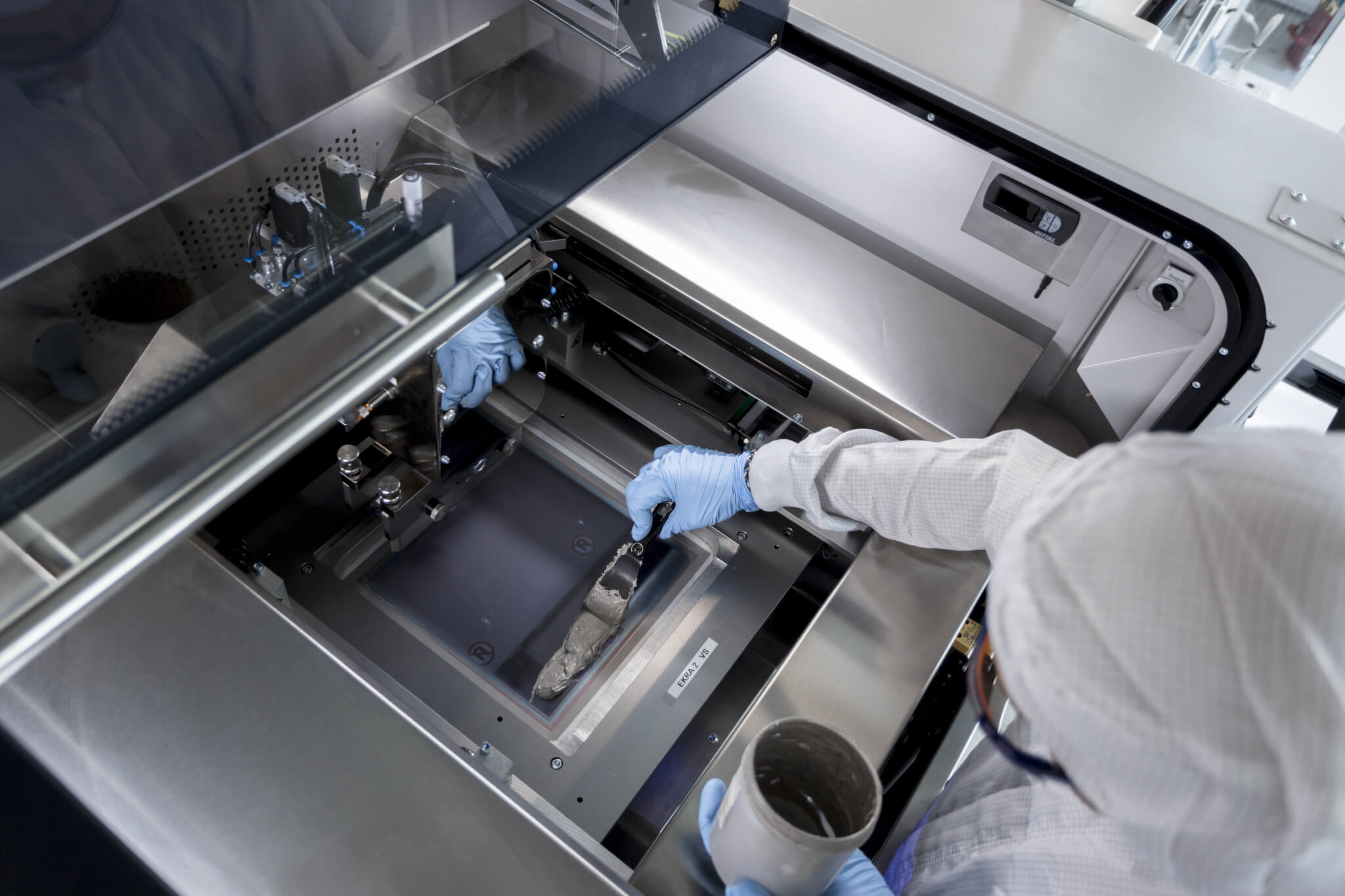
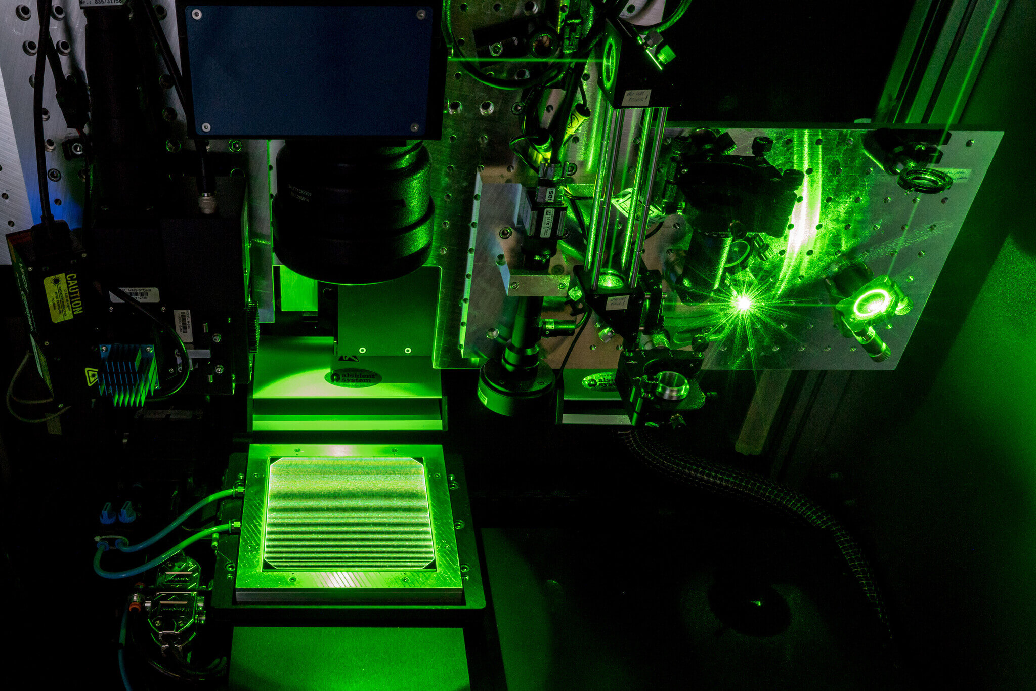
Laser and printing technologies play a central role in the production of industrial solar cells, especially in structuring and metallization.
In addition to flatbed screen printing, the focus is also on alternative printing processes such as stencil and rotary printing, dispensing and flextrail processes as well as inkjet processes. We are continuously working on process development to realize the finest contact structures with the aim of gradually reducing high-priced silver. Central components such as print heads are developed in-house and evaluated in existing systems, and development work in the area of printing forms and printing media is addressed. Furthermore, Fraunhofer ISE has broad expertise in process simulation and digitization as well as in thermal and photonic processes for drying and sintering printed structures.
Laser processes are established in photovoltaics for marking, cutting, drilling, doping, "defect" and "layer" annealing, cell interconnection and layer structuring, for example, or are the subject of research and development. Depending on the application, the aim is to save material or increase the efficiency of the solar cells. At Fraunhofer ISE, these micromaterial processing methods are continuously developed, optimized, modeled and simulated in coordination with upstream and downstream production steps.
Furthermore, we develop and demonstrate system technology for precise high-throughput laser processing of current and future wafer formats in order to realize the smallest structure sizes. In addition to crystalline silicon photovoltaics, our work addresses III-V solar cells, thin-film photovoltaics and the processing of semiconductors for power electronics.


