| Duration: | June 2015 - May 2017 |
| Contracting Authority/ Sponsors: | European Union’s Horizon 2020 research and Innovation programme under the Marie Sklodowska-Curie grant agreement N° 655272 |
| Project Focus: |
HISTORIC – High Efficiency GaInP/GaAs Tandem Wafer Bonded Solar Cell on Silicon


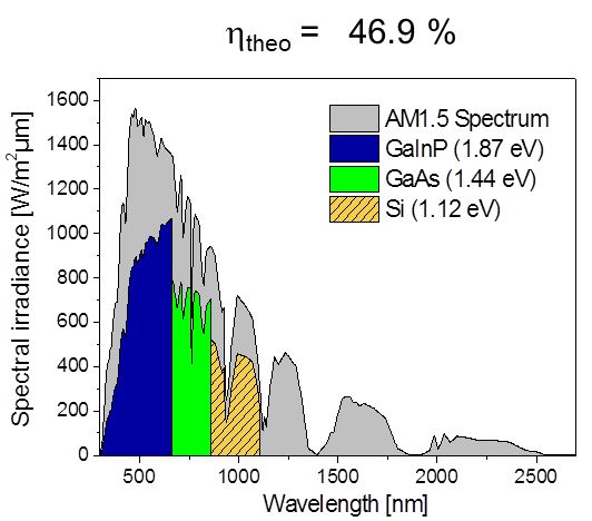
The direct conversion of photons into electricity is a promising clean energy solution to answer the multiple challenges of energy supply security, competitiveness, electricity prices and climate change. Monocrystalline silicon (c-Si), the dominant technology on the photovoltaic market, benefits from a well-established industry and record power conversion efficiency around 26 %. Mainly limited by its inherent material properties, however, c-Si technology, has very little room for efficiency improvement. On the other hand, much higher solar cell efficiencies have been achieved by stacking subcells of III-V semiconductor material to create so-called multi-junction solar cells. At present, however the III-V solar cells are restricted to specific markets (space and terrestrial concentration) for cost and availability reasons. A hybrid solution combining the advantages of III-V multi-junction solar cells with the benefits of Si, the most wide-spread photovoltaic material, offers great opportunities. Indeed, conversion efficiencies above 46 % (under 1-sun AM1.5G conditions) can be theoretically expected (see fig. 1) for a triple-junction device based on conventional c-Si cells combined with additional GaAs and GaInP p-n junctions (3-5 μm of III-V material on top of a silicon wafer).
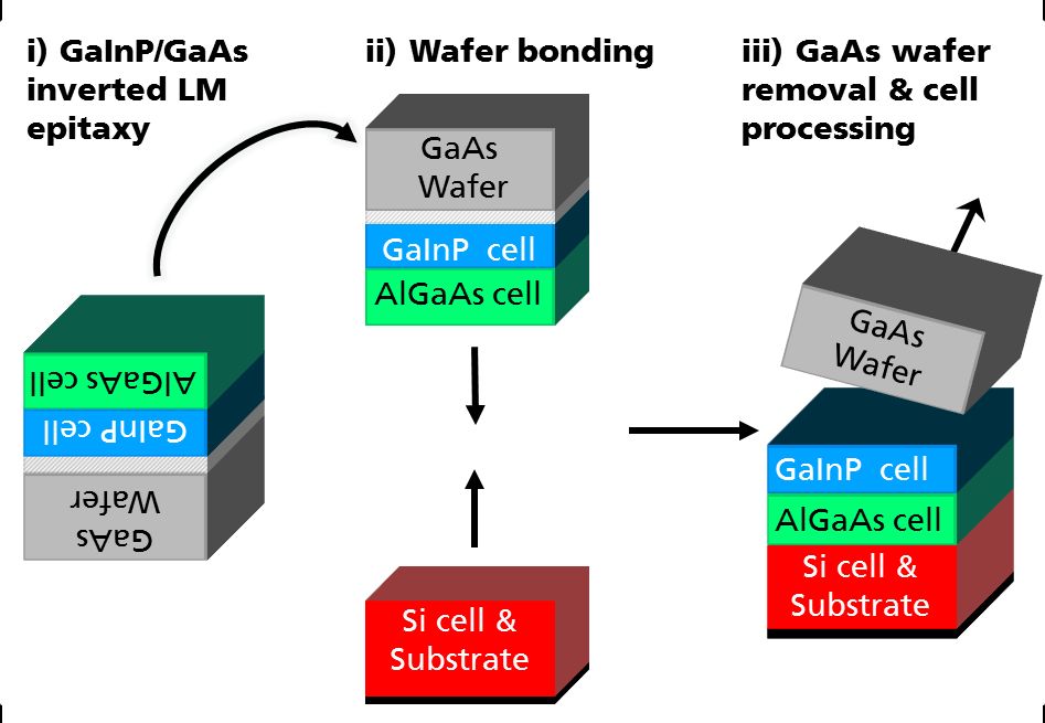
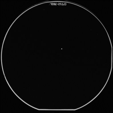
In the practice, however, there are still hurdles to overcome. The direct epitaxial growth of GaAs and GaInP on Si is highly mismatched and sufficient material quality has not been achieved so far. The innovative approach proposed in this project bypasses the mismatch and enables high crystal quality III-V compounds to be bonded with Si through surface activated wafer bonding: III-V layers are grown lattice-matched on GaAs and then bonded to Si, followed by substrate removal (see fig. 2). In addition, the surface activated wafer bonding produces excellent yields over 4” wafer areas as shown in fig. 3.
The objective of this research project is to produce the large scale (4cm2) Ga0.51In0.49P/GaAs//Si triple-junction solar cells with an efficiency exceeding 30 % at one sun AM1.5G spectrum. This requires: i) electro-optical simulations to find the optimum layer parameters and light trapping features to achieve a perfectly current matched structure ii) to grow lattice-matched high quality Ga0.51In0.49P/GaAs on GaAs tandem top cells and independent Si cell processing iii) to study, understand and realize large scale GaAs/Si bonding interfaces with outstanding material and electrical properties iv) to process and characterize the final multi-junction device. This project aim is the world record III-V//Si solar cell above 30 % efficiency.
Related Links:
- News: 31.3 Percent Efficiency for Silicon-based Multi-junction Solar Cell
- Press Release: 30.2 Percent Efficiency – New Record for Silicon-based Multi-junction Solar Cell
- Journal Article: Monolithic Two-Terminal III–V//Si Triple-Junction Solar Cells With 30.2% Efficiency Under 1-Sun AM1.5g (publica.fraunhofer.de)