| Duration: | 04/2021 - 03/2024 |
| Contracting Authority/ Sponsors: | Bundesministerium für Bildung und Forschung (BMBF) (Fkz. 01DM21006A) |
| Project Partners: | AIXTRON, Broadcom National Research Council, Optiwave, University of Ottawa |
| Project Focus: |
AIIR-Power
AI-assisted design and fabrication of photonic infrared power converters for energy and telecommunication
Photonics and optoelectronics are key technologies for the digitalization. The design of corresponding semiconductor devices as well as the modeling of epitaxial processes can still benefit significantly from artificial intelligence (AI) methods in the context of Industry 4.0. Ubiquitous digitization and automation, as well as the Internet of Things, require constant energy and data streams. The emerging technology of photonic power transmission, also known as power-by-light enables power and data transmission to be combined in a single optical link. By using optical telecommunication wavelengths around 1.5 µm, the applications of such power-by-light systems can be extended to remote locations, enabling unlimited remote power supply. AI-assisted approaches to photonic power converter (PPC) design and fabrication are critical for further cross-industry application of photonic power and data transmission.
The German-Canadian collaborative project "AIIR-Power" aims at the development of AI techniques for the optimization of optoelectronic device designs and their epitaxial fabrication, as well as their application for the realization of PPCs for telecommunication wavelengths around 1550 nm. The main objectives of the consortium include:
- O1) AI design approach: development and implementation of machine learning methods for dimensionality reduction in optoelectronic device design using PPCs as an example.
- O2) Smart epitaxy process: develop and implement AI-assisted modeling of the epitaxy process and investigate reinforcement learning algorithms for real-time control systems to improve material quality and cost effectiveness and prepare for Industry 4.0.
- O3) Demonstration of AI-enhanced PPC devices: Design and fabrication of new multi-junction PPC devices for telecommunication wavelengths around 1550 nm with increased output voltage.
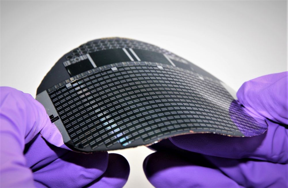
At Fraunhofer ISE, innovative PPC photovoltaic cells based on the III-V semiconductor material InGaAs(P) are developed within the project. This represents an optimal absorber material for the widely used telecommunication wavelengths. In particular, multi-junction PPCs are being developed for laser wavelengths in the optical C-band around 1550 nm with up to ten vertically stacked subcells. The subcells, which are serially interconnected via tunnel diodes, allow the output voltage of a single InGaAs(P) photovoltaic cell to be multiplied to, for example, 3 to 5 V. This avoids the necessity for a lossy upconversion of the voltage for the operation of downstream electronic applications.
In addition to material development and epitaxial layer fabrication, a thin film process technology for InP based semiconductor devices is being developed. Furthermore, so-called engineered substrates are being developed, with which cost-intensive InP substrates can be replaced by lower-cost GaAs.
First important project results include the model-based investigation of the InGaAsP material system for the target application, 10-junction InGaAs PPCs with an output voltage >5 V, the implementation of transparent tunnel diode structures on InP with peak current densities above 75 A/cm², as well as the adaptation of our thin film technology to InP substrates and first InGaAs thin film PPCs with backside mirrors.

