| Duration: | October 2010 - September 2013 |
| Contracting Authority/ Sponsors: | EU |
20plμs – Development of a Slurry-Based Wire-Sawing Process: Structured Wires


Most of the solar cells around the world are based on wafers which are produced from silicon crystals by wire-sawing. In the wire-sawing process, the crystal is pressed against several hundred wire loops and sawn into wafers with the help of an abrasive medium. Our further development of this sawing technique involves investigating the use of structured wire instead of the straight wire currently used. The structured wire enables higher feed rates and thus significant cost savings for the wire-sawing process. Our investigations concentrate on the effect of process parameters, which determine the wafer geometry and throughput decisively.
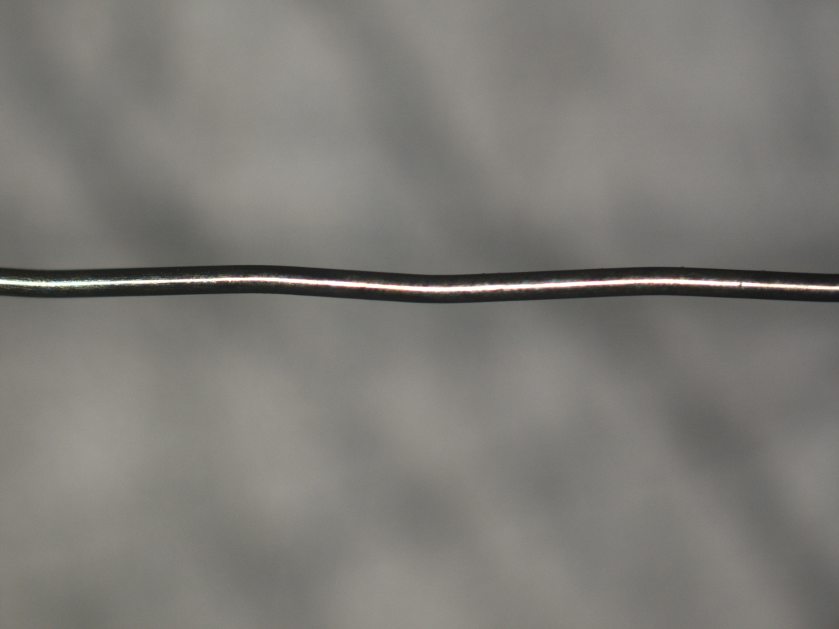
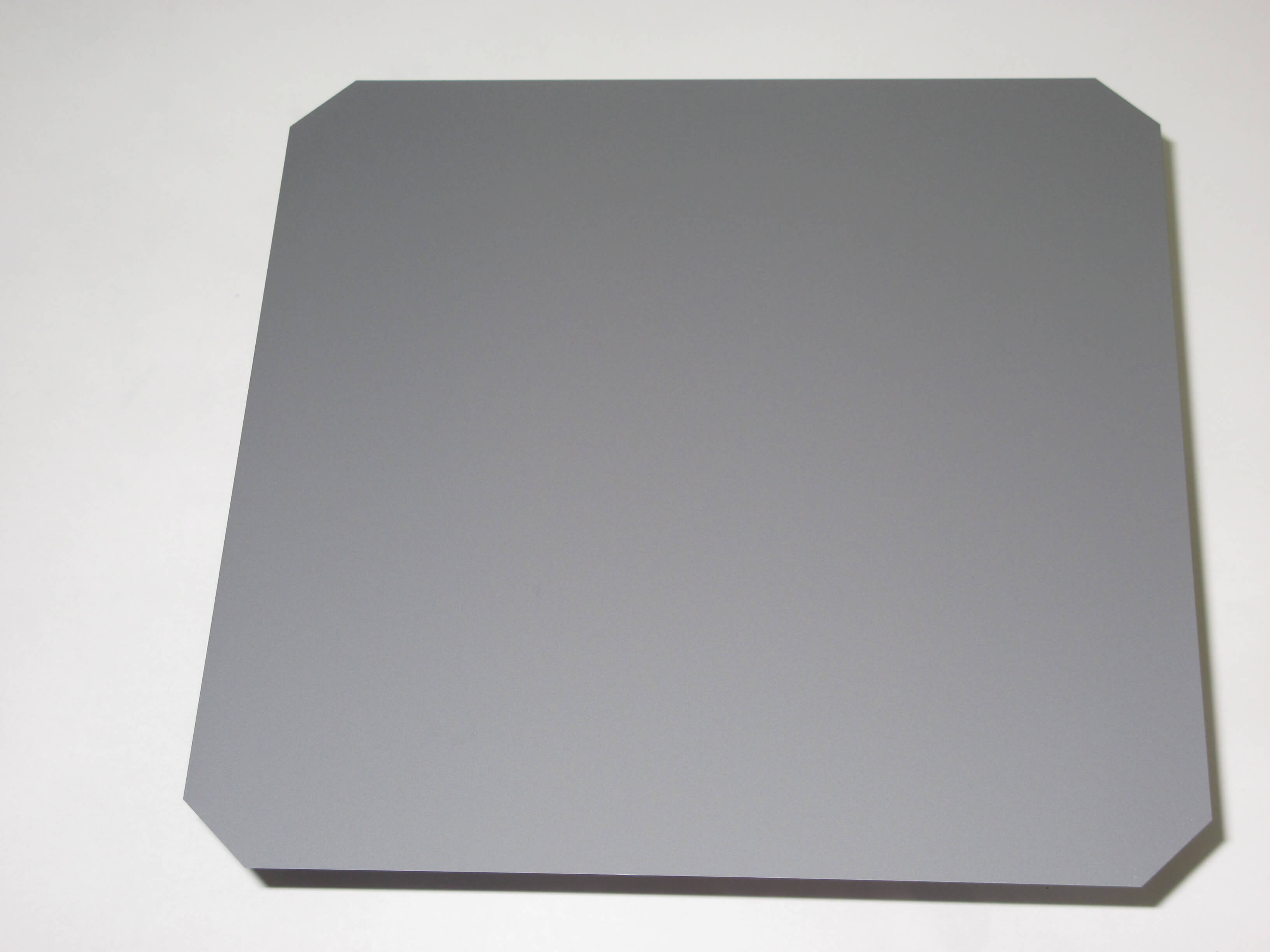
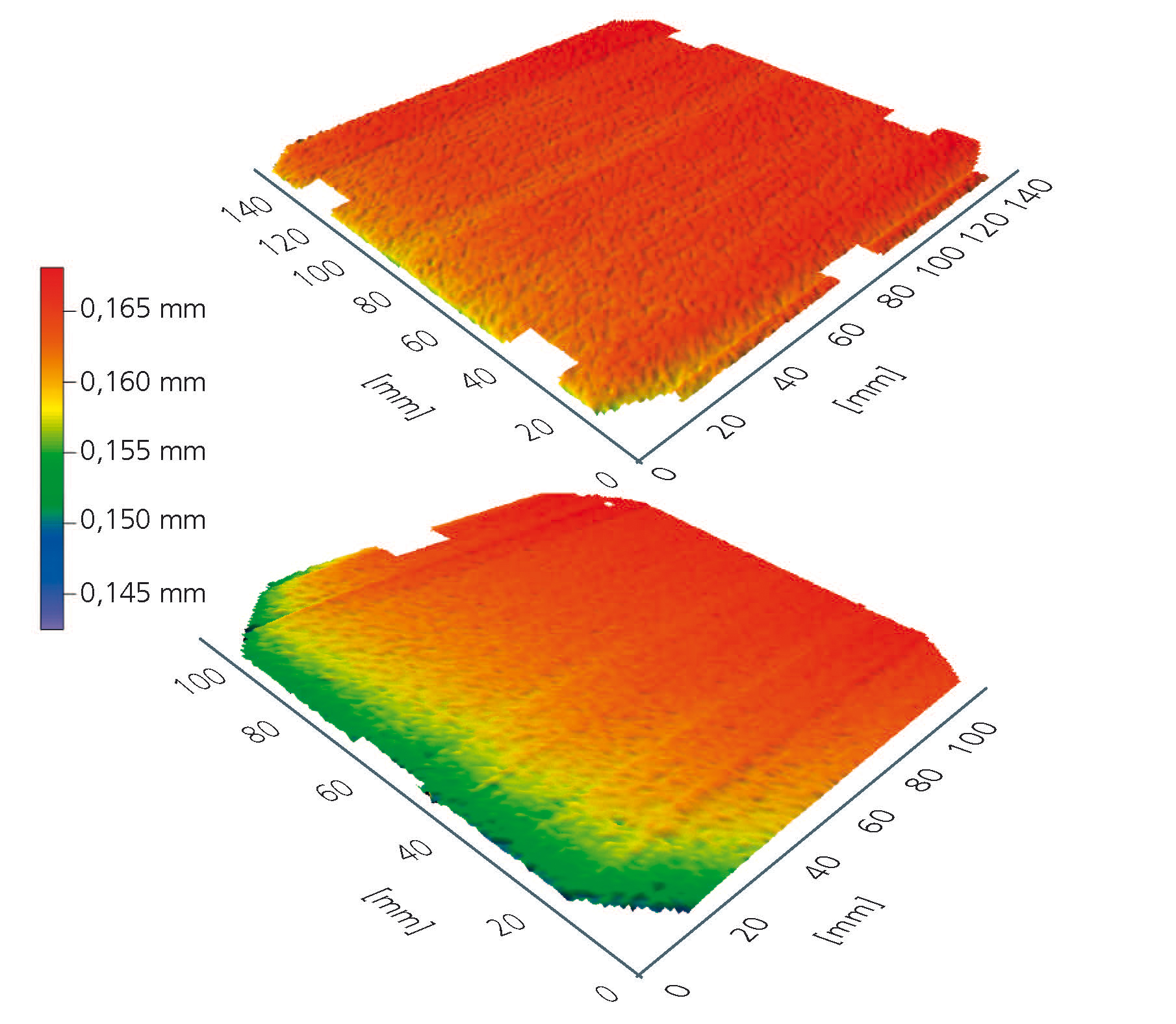
The standard, industrially applied sawing process, which is based on the use of a silicon carbide slurry and straight steel wire, has the disadvantage that the wafers are wedge-shaped after sawing. By using structured wire, we were able to produce wafers which have a more uniform thickness over the entire area and thus have a much less pronounced wedge form. Structuring the sawing wire (Fig. 1) ensures that the slurry enters the groove more efficiently, resulting in a more stable sawing process, so that no sawing marks or inhomogeneities are visible on the wafer surface (Fig. 2). In addition, the processing time is significantly shortened, as the sawing efficiency is increased by the wire structure, allowing higher feed rates. With the structured wire, we achieved a reduction of up to 50% in the thickness variation over the wafer area, accompanied by an approximately 30% higher feed rate compared to straight wire (Fig. 3). A further advantage is that the currently used slurry saws need to be only slightly modified to accept structured wire. These advantages apply to the sawing of both monocrystalline and multicrystalline silicon. Thus, the structured sawing wire is ideally suited to achieve significant cost savings with existing equipment while simultaneously improving wafer quality.
In the course of the project of 20plμs, the topics of "Wire Wear" (Annual Report 2011) and "Thin Wafers" (Annual Report 2012) were also addressed.