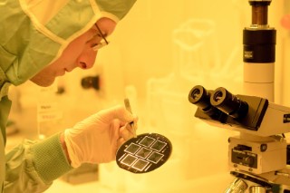
The Fraunhofer Institute for Solar Energy Systems ISE has set a new efficiency record for silicon solar cells. For the first time, an efficiency of 25.1 percent has been measured for a both sides-contacted silicon solar cell. Having a simple rear side contact without any patterning, this type of solar cell converts one quarter of the incident sunlight into electricity. The new concept for the solar cell rear side holds great potential for further increases in efficiency.
more infoPress Releases
-
Press Release #26 / 2015
20% Efficient Solar Cell on EpiWafer
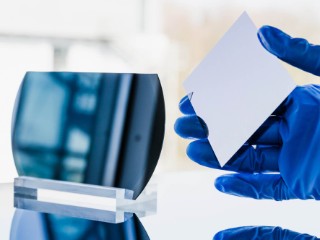
Recently NexWafe GmbH was spun out of the Fraunhofer Institute for Solar Energy Systems ISE, in order to bring the Institute’s kerfless EpiWafer technology to the market and rapid commercialization. In the EpiWafer technology, a thick crystalline silicon layer is epitaxially deposited and subsequently detached after growth to produce a freestanding wafer of standard thickness. Due to the radical changes in the manufacturing value chain, EpiWafers can be produced at an appreciably lower cost compared to the traditional wafer manufacturing process. The EpiWafer is a direct substitute for conventional n- or p-doped silicon mono-crystalline wafers.
more info -
Presseinformation #24 / 2015
Fraunhofer ISE Has Developed a New Generation of Reference Cells – Optimized Structure Allows the Calibration of the Expanded Infrared Spectrum
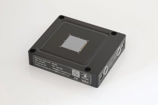
Scientists at the Fraunhofer Institute for Solar Energy Systems ISE have developed a new version of reference cells for calibrating solar cells. At the institute’s calibration laboratory, a new cell type based on negative, conductive silicon material (n-type), was incorporated while the structure of the reference cell was optimized. For the calibration of different types of solar cells, the reference cell’s spectral response can be accurately adjusted using optical filters, thereby significantly reducing any measurement uncertainty. The new version of the reference cells meets all international standards (World PV Scale and IEC 60904-2). The new cells will allow test laboratories and cell and module manufacturers in particular to significantly improve the quality of their measurements. The outdoor version of the cell also makes it possible to take exact measurements of solar insolation in the field.
more info -
Presseinformation #23 / 2015
Fraunhofer ISE Develops Highly Compact Inverter for Uninterruptible Power Supplies – Silicon Carbide Components Enable Efficiency of 98.7 percent
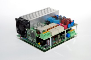
Researchers at the Fraunhofer Institute for Solar Energy Systems ISE have developed a highly compact and efficient inverter for use in uninterruptible power supplies (UPS) for electrical devices. The demonstrator, which contains innovative silicon carbide components, was developed in cooperation with an industry partner and achieved an efficiency of 98.7 percent. The research and development findings can be applied to other areas of electronic power conversion in which weight and efficiency play a key role, e. g. electric mobility or portable power supply.
more info -
Press Release #22 / 2015
»Solar for All« contest focuses on solar village and mini-grid solutions – Fraunhofer ISE and Canopus Foundation start second edition of the award

Solar power gained from photovoltaics (PV) will soon be the cheapest form of electricity in many regions of the world, as a recent study on long-term scenarios by Fraunhofer ISE on behalf of Agora Energiewende shows. In sunnier regions, for applications in rural areas, one kilowatt hour (kWh) gained from solar energy already today is cheaper than a kWh produced by a diesel system, which is due to the fast growing global market for PV. In this context, the Fraunhofer Institute for Solar Energy Systems ISE and the Canopus Foundation will put the focus of the second »Solar for All« contest on solar village and mini-grid solutions and their highly recognized potential for rural development. Further information on submission criteria will be released late 2015.
more info -
Press Release #21 / 2015
Heat pumps and chillers: highly efficient components of our future energy supply – Fraunhofer ISE opens new test and development center
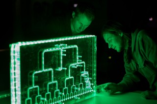
The Fraunhofer Institute for Solar Energy Systems ISE has opened its new test and development center for heat pumps and chillers in Freiburg, thus doing justice to the central importance of these technologies in the energy transition. The Institute offers industry completely new possibilities to have their components, devices and entire systems developed and tested to ensure highly efficient heating and cooling performance.
more info -
Presseinformation #19 / 2015
Keep cool – cooler batteries are safer and live longer – Fraunhofer ISE inaugerates its new location for battery system technology
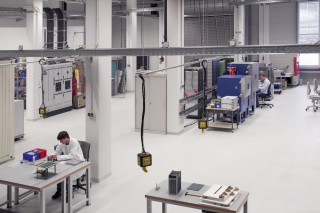
The Fraunhofer Institute for Solar Energy Systems ISE is bundling its research activities in the field of battery systems in a new laboratory. Together with its partners, it offers the industry a unique array of services: from investigations of single battery cells through the development of complete battery systems up to the optimal integration of entire storage systems in different applications with respect to both power and communications technology. The researchers use the laboratory to investigate, among other things, the thermal behavior of battery cells and modules using a highly precise calorimeter. The results enable battery systems with maximum safety, long lifetime and high power efficiency to be developed.
more info -
Presseinformation #20 / 2015
Megawatt-Wasserelektrolyseure – die guten Geister der Energiewende – Fraunhofer ISE eröffnet neues Labor in Freiburg
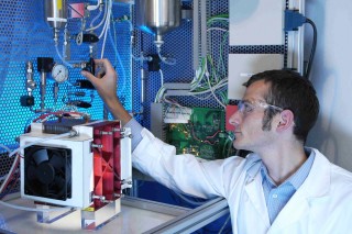
Das Fraunhofer-Institut für Solare Energiesysteme ISE weiht sein neues Labor für Wasserelektrolyseure in Freiburg ein. Damit wird es möglich, Anlagen im Megawatt-Leistungsbereich zu untersuchen und zu charakterisieren. Die auch am Institut entwickelten Polymerelektrolytmembran- (PEM-) Elektrolyseure lassen sich extrem schnell regeln, so dass fluktuierende Stromerzeugung aus regenerativen Energien netzdienlich zur Wasserstofferzeugung für die Mobilität, aber auch für die Energiespeicherung genutzt werden können. Anlagen dieses Typs könnten die Problematik des geplanten Netzausbaus zeitlich entschärfen.
more info -
Press Release #18 / 2015
Storage and heat transformation technologies – important pillars of the energy transformation – Fraunhofer ISE expands range of research and development with new site
Since being founded more than 30 years ago, the Fraunhofer Institute for Solar Energy Systems ISE has covered a wide range of complementary technologies, optimally preparing it for the challenges facing the energy transformation. In addition to solar technology research, the systemic aspects and questions regarding energy storage also played a role right from the start. Today energy storage technologies and efficient heating and cooling processes are two topics particularly in the focus of the energy transformation. Fraunhofer ISE has now consolidated its activities in these areas at its new site on the Auerstrasse in Freiburg. The new location offers much more space which has allowed the Institute to significantly expand its laboratory equipment. On July 2, 2015, the new center for storage and heat conversion technologies was officially inaugurated in the presence of representatives from several German federal ministries as well as from industry associations and the industry itself.
more info -
Press Release #16 / 2015
Fit for the Energy System of the Future – European Project Team Presents Planning Tool for the Distribution Grid
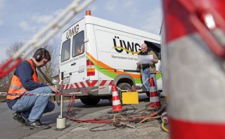
Due to the rising penetration of photovoltaics, heat pumps and electric vehicles (EV) in the power distribution grid, the requirements for grid flexibility and stability are increasing. Just how existing power grids can be made fit for the future was the topic of a cooperative German, Danish and Dutch project in which the Fraunhofer Institute for Solar Energy Systems ISE was involved. Over a period of three years, the project partners from research and industry took well-proven techno-economic modelling and optimization tools and implemented them into the new NEMO tool suite. This forward-looking tool prepares the distribution grid for the energy system of the future, by predicting the interaction between decentralized suppliers and consumers in realistic future scenarios. After the test phase was successfully completed in all three countries, a workshop was held to present the capabilities and advantages of this new tool to distribution and transmission grid operators as well as associations, grid service providers and system operators.
more info
