| Duration: | April 2013 - March 2015 |
PV-NIL
Nanoimprint Lithography for Extremely Fine Solar Cell Structures


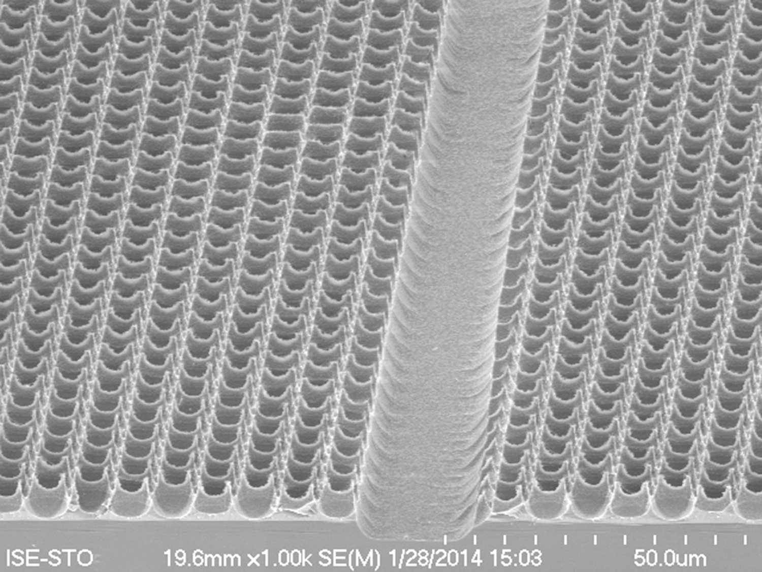
The miniaturization of components is important for photovoltaics. We are investigating nanoimprint lithographic (NIL) processes in order to produce e. g. extremely fine structures for photonic textures or very narrow contact fingers with well-defined morphology. To this purpose, we are using a new high-end facility, which is integrated into a mask aligner for classic photolithography. There, we are able to develop new processes under very well defined conditions, which we then transfer to specifically developed roller NIL equipment.
Although the structural resolution required in photovoltaics is clearly coarser than in microelectronics, new features applying NIL processes are also conceivable there. They combine the properties of extremely fine structural resolution, which are otherwise possible only with complicated electron-beam scribing, with large-area replication with very high throughput such as roll-to-roll processes. Integration of the new NIL tool from the EVG company into a mask aligner meant that very diverse, finely resolved structures, which previously had been possible only on small areas in the laboratory, could be integrated into products. To produce the master structures, we use a combination of various lithographic processes such as interference lithography, NIL, hot embossing and photolithography, as well as anisotropic etching processes. Embossing stamps can then be replicated from the master structures, so that many different characteristics can be reproduced in a single NIL step.
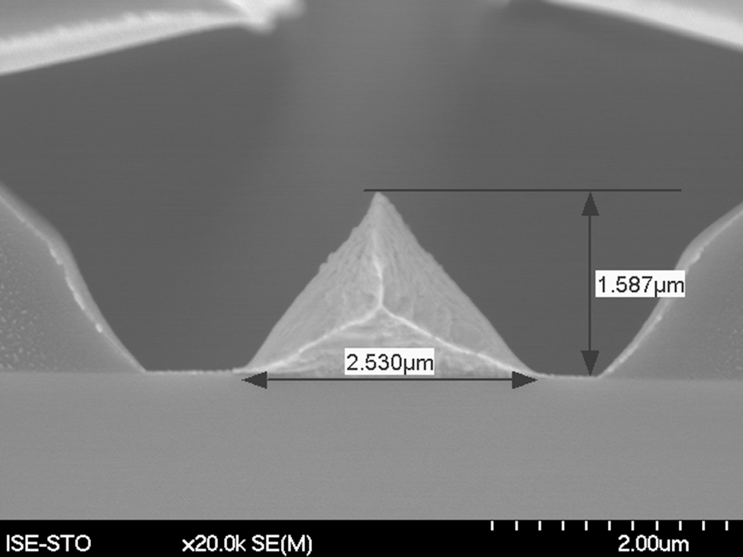
In the Fraunhofer ”PV-NIL“ project, we are investigating etching masks which unite the morphology for an efficient texture and the finest contact fingers. We are also investigating the production of finest contact fingers with a prismatic crosssection, in order to minimize the effective shading.