| Duration: | 02/2023 - 01/2026 |
| Contracting Authority/Sponsors: |
Bundesministerium für Wirtschaft und Klimaschutz (BMWK), PtJ |
| Project Partners: | LPKF SolarQuipment GmbH, Asphericon GmbH, Robust AO GmbH, Raylase GmbH, RENA, Technologies GmbH |
| Project Focus: |
Miracle – High-Throughput Microablation for Electroplating Next-Generation Solar Cells
The growing market for galvanically metallized (plating) solar cells requires innovative technology in the field of laser structuring - a higher resolution for smaller conductor paths, a large processing field for growing wafer formats and faster beam deflection for shorter process times. In "Miracle", Fraunhofer ISE and five industrial partners are coming together to jointly develop and build new system concepts that will make laser structuring for plating more economical and competitive and thus enable high silver savings in solar cell production.
The scarcity of silver resources and the rapid development of new solar cell types such as HJT, TOPCon and perovskite and, above all, the constantly growing wafer formats pose new challenges for the common metallization techniques. Copper-based metallization using electroplating is gaining in importance and market share. It enables drastic silver savings, higher efficiencies for new cell types and a reduction in the minimum TOPCon layer thickness required. In production, plating is preceded by a laser-based opening of the anti-reflective coating. The size, homogeneity and quality of the laser structure significantly determine the contactfinger width, the contact and series resistance as well as the recombination and adhesion properties and therefore also the success of the plating technology. Here, the current status of laser systems (structure size 15 μm to 20 μm, format ≤168 x 168 mm², throughput ≤7500 wafers per hour) is far removed from future market requirements.
Results from Fraunhofer ISE show an absolute increase in efficiency of 0.65% if the opening size is reduced from 14 μm to 5.5 μm. Additionally, the throughput should even increase further despite the larger formats and a smaller opening. The aim of the project is therefore to replace established compromise solutions with a new system design and thus establish a previously unattained specification in a pilot system which
- produces homogeneous laser openings apertures with a width of less than 10 μm,
- can process M12 format wafers
- and achieves a throughput of 8000 wafers per hour.
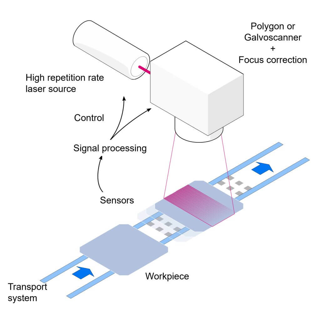
Solutions for this are based on ultra-fast scanners, a new optical design, active focus correction, fast control and the networking of components with a high bandwidth.
