| Duration: | September 2015 - February 2019 |
| Contracting Authority/ Sponsors: | German Federal Ministry of Education and Research (BMBF) |
| Project Partners: | Technical University Ilmenau , Philipps University Marburg, Aixtron SE |
| Project Focus: |
MehrSi – High-Efficiency III-V Multi-Junction Solar Cells on Silicon


III-V multi-junction solar cells currently achieve up to 38 % AM1.5g efficiency for the conversion of sunlight into electricity. Common silicon solar cells cannot achieve such high conversion efficiencies. However, the costs of III-V semiconductors are still too high to justify the use in flat plate photovoltaic modules. For this reason, this project investigates the combination of III-V and silicon technologies by depositing thin III-V semiconductor layers directly on a silicon pn-junction. Based on that, we develop multi-junction solar cells that can achieve efficiencies greater than 30 %.
In the “MehrSi” project funded by the German Federal Ministry of Education and Research (BMBF), we develop tandem solar cells made of III-V semiconductors and silicon. Here, the sunlight is divided into two or even three spectral ranges and absorbed in Si as well as III-V materials, such as GaInP or GaAsP. This leads to a higher theoretical efficient conversion efficiency of sunlight into electricity. We develop processes enabling direct growth of the III‑V layers on a Si bottom cell. Here, it must be ensured that the silicon solar cell does not degrade due to the III-V growth. Furthermore, the transition between silicon and the III-V semiconductors, as well as the transition in the lattice constant (atom distance in crystal) between the materials must be realized. Together with Technical University Ilmenau, we investigate the interface between Si and GaP and try to achieve a low defect density. Together with Philipps University Marburg, we optimize the transition layers in the lattice constant between the Si and the GaInP and/or GaAsP solar cells. The focus here is to intentionally create misfit dislocations in the plane and to relax the crystal purposefully without causing extended defects that propagate throughout the III-V solar cells. Together with Aixtron, we further develop growth conditions to enable cost-effective production through a high growth rate of up to 100 µm/h.
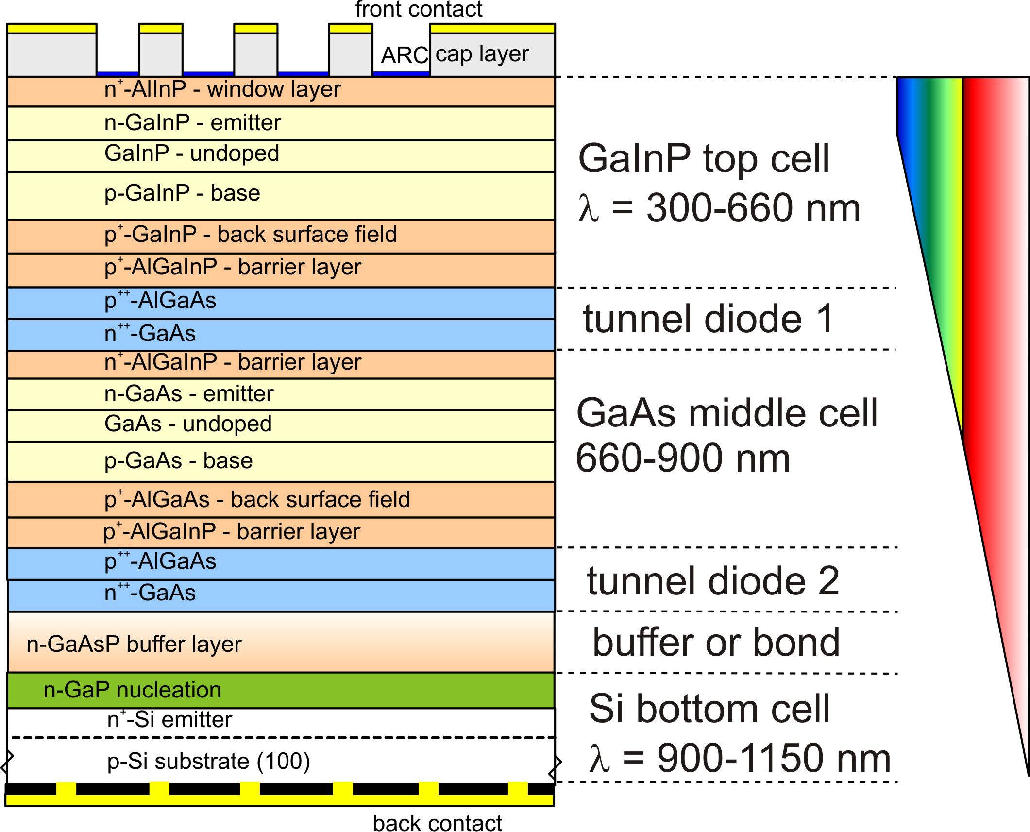
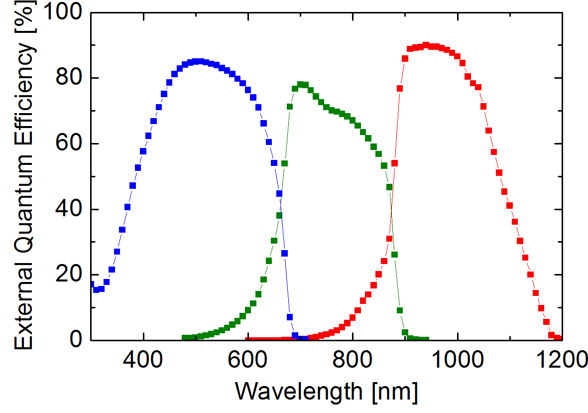
We made already significant progress in 2016 and could demonstrate a directly grown triple-junction solar cell on silicon (Fig. 1). The solar cell has an efficiency of 19.7 % under the AM1.5g spectrum. The quantum efficiency is shown in Fig. 2 and illustrates the division into the three sub-cells made of GaInP, GaAs, and Si. The top III-V solar cells still show a high defect density in the range of 108 cm-2. We are currently working on achieving better results. In that case, efficiency levels of more than 30 % can be achieved.