| Duration: | June 2016 - September 2019 |
| Contracting Authority/ Sponsors: | German Federal Ministry of Economic Affairs and Energy (BMWi) (BMWi) |
| Project Partners: | KSG GmbH, Koenen GmbH |
| Project Focus: |
KAluS50 – Cost-Beneficial Aluminum Metallization for Solar Cells and Circuit Boards


The project focuses on novel printing processes for the electrochemical structuring of metal layers (e.g. Al, Cu, Ni, Ti) which offer advantages in the solar cell industry and also in other areas such as the circuit board industry. For photovoltaics, structuring processes of metal layers are particularly interesting for interdigitated-back-contact (IBC) solar cells. Currently used processes, in which usually etch resists are used and the metal is subsequently chemically etched, are complex and expensive. The process developed in the project enables local etching of different thin metal layers and layer stacks within seconds, which makes the process flexible and cost-effective compared to reference processes.
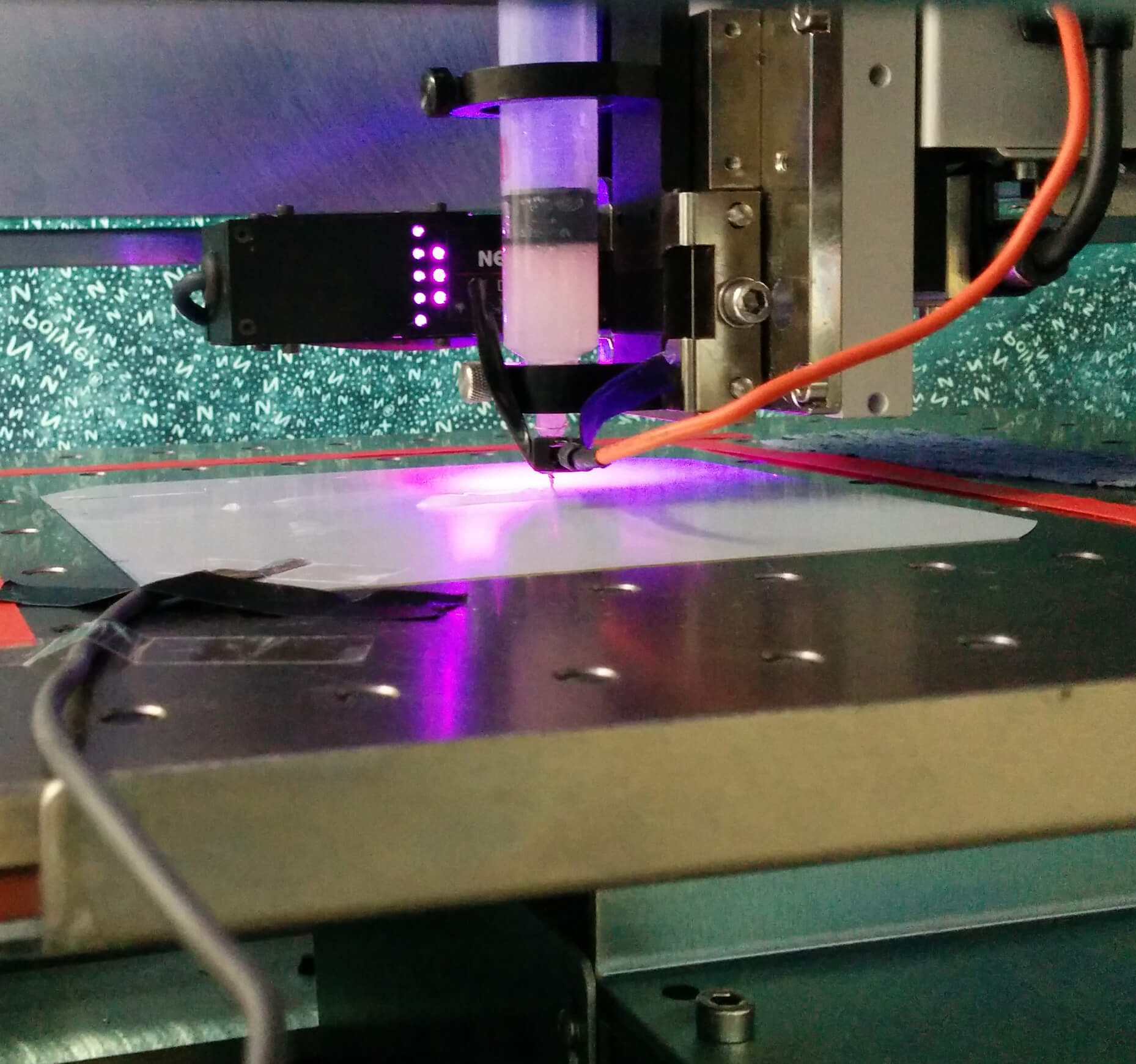
The process principle is known from Electrochemical Machining (ECM) and is used for local structuring here. A pasty electrolyte is applied to ensure local, anodic dissolution of the metal layer. In order to realize electrochemical structuring on larger surfaces, the screen printing and dispensing processes are used. These printing processes not only serve to transfer the necessary medium to the metal surface to be structured but also to locally close the current circuit during the printing step. The metallic screen mesh or the dispenser nozzle represents the cathode. The etch rate can therefore be directly adjusted by selecting the electrical parameters, thus enabling good control and short process times. For applications where high lateral conductivity of the generated metal pattern is required (e.g. IBC solar cells), these structures can be additionally thickened by plating.
Main project tasks are:
- Further development of the process with regard to width and depth of the etching line, as well as to electrical contact separation
- Optimization of the printing paste with regard to printability and electrically supported etching properties
- Conversion of commercial dispenser and screen printing systems for electrochemical etching
- Use of electrochemical structuring by dispensing and screen printing on solar cells and circuit boards
- Post-treatments for electroplating
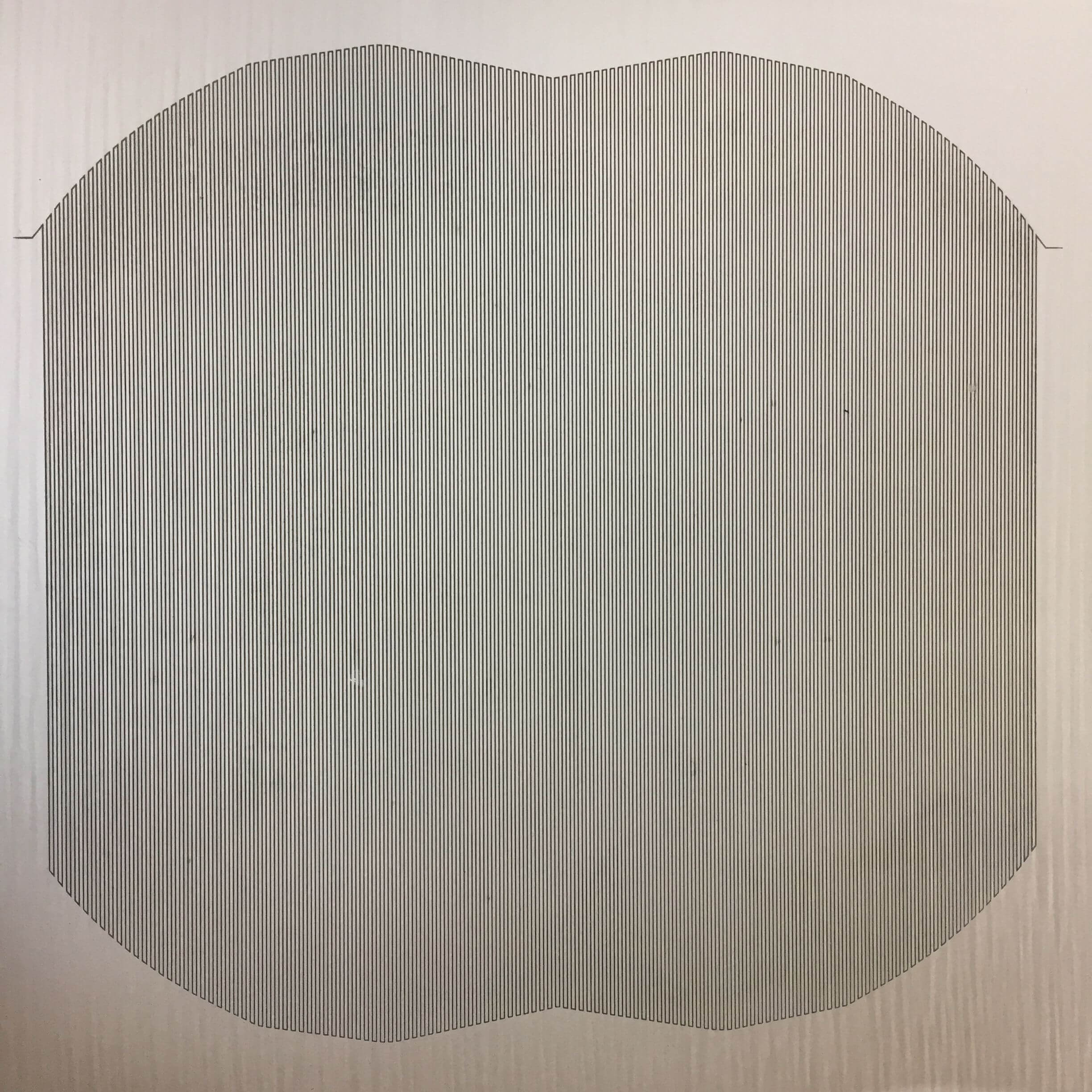
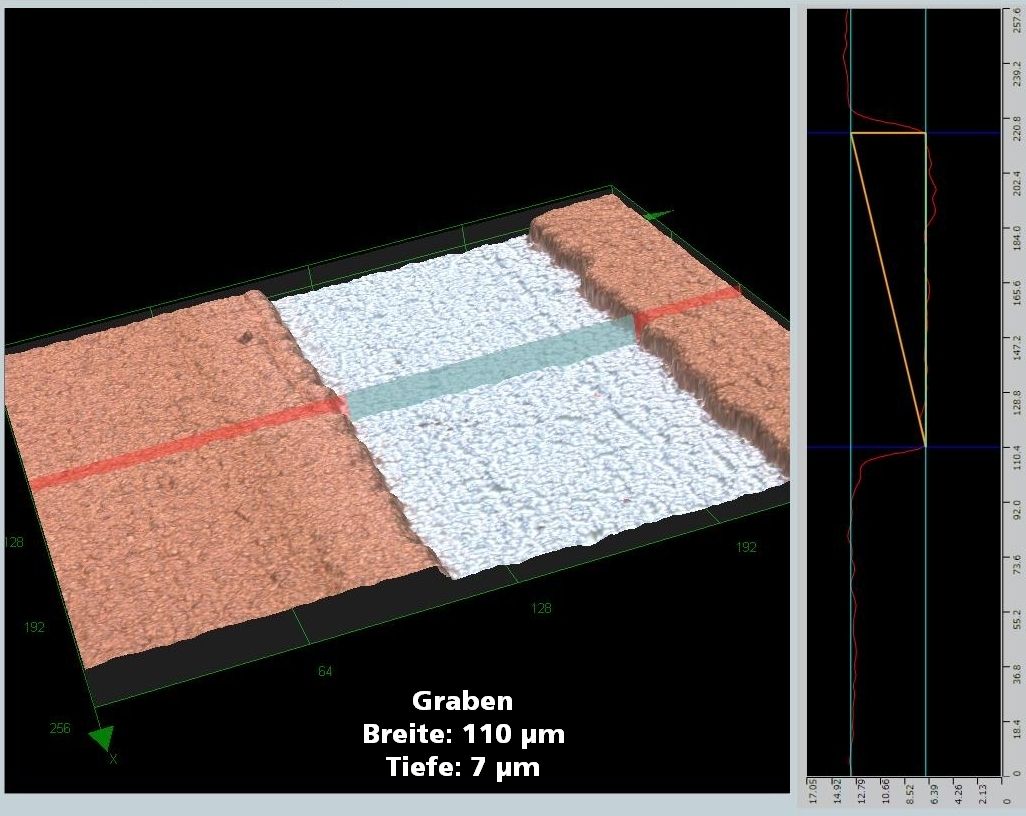
In the course of the project to date, electrochemical screen printing has already made interdigitated structures on an area of 125x125mm² from a 100nm thick aluminum layer (Fig. 1). In addition, it was possible to structure individual layers in layer stacks. For example, a 50nm copper layer could be selectively removed from the 100nm thick aluminum layer underneath. Such a structure was then plated with copper. In this case, the aluminum area serves as protection layer against galvanic deposition due to its self-passivation, whereby the aluminum trench is retained and the thin copper layer can be selectively grown (Fig. 2). Through a subsequent short etching step, the aluminum layer can be selectively removed in the intermediate area, turning the copper areas into electrically isolated conductor tracks that can be used for solar cells, circuit boards and other electrical components.