| Duration: | April 2014 - March 2015 |
| Contracting Authority/ Sponsors: | Self-funded Research Project |
| Project Focus: |
iPorSi – Development of Nano-Porous Silicon Layers in an Inline Process


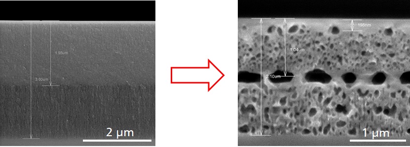
Epitaxially grown and detached thin silicon layers for photovoltaics have cost savings potential of more than 50 % and are thus of high interest. In addition to silicon absorber deposition, the nucleation and removal layer consisting of porous silicon is the most important new process. Until now, this process based on electro-chemical etching in hydrofluoric acid / ethanol was only performed on single wafers. No systems are available today for a throughput of several thousand wafers per hour, which hinders the industrial introduction of epitaxial wafers dramatically. For this reason, the objective of the “iPorSi” project is to establish porosification processes for this Si detachment concept on a prototype inline system.
The necessary porosification process for the production of epitaxially grown and detached thin layers and the development of an industrial high-throughput technology was successfully realized by Fraunhofer ISE within the scope of the “iPorSi” project on a prototype etch system. After adjustment and commissioning of the etch system and identification of suitable wetting agents, we modified multi-layer porosification layers on 500 µm thick mono-crystal silicon wafers such that after reorganization in hydrogen and subsequent Si epitaxy, a controlled detachment process takes place. In addition to process parameter adjustment for the provision of an optimum epitaxy template and controlled removability, re-usability of substrates was investigated and the process stability improved.
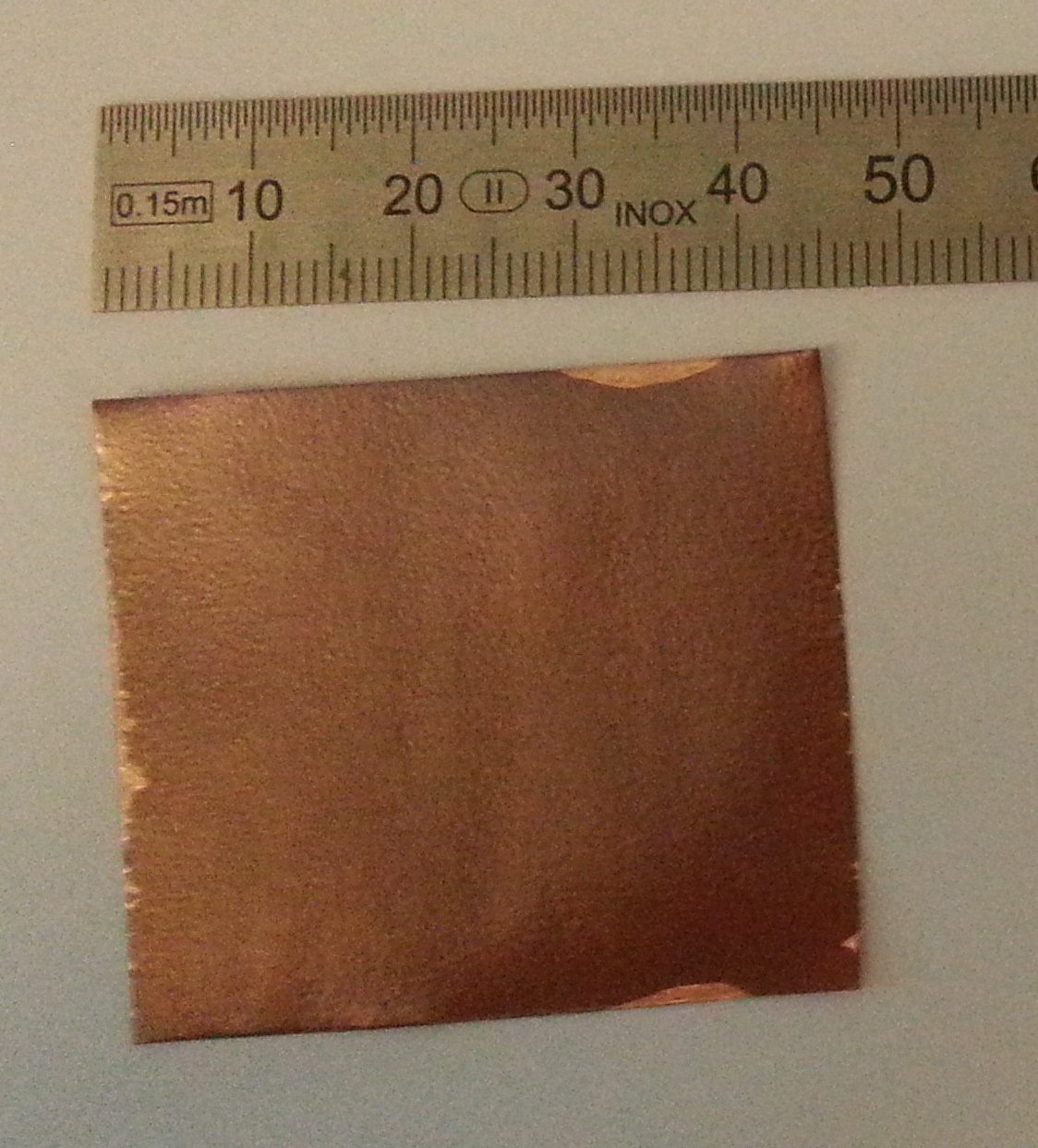
In a next development step, we produced several µm thin (< 10 µm) macro-porous Si foils that could be directly detached without further process steps, i.e., also without reorganization (45x45 mm²). These macro-porous foils were then adhered onto the carrier substrate using an in-house developed oxidic SolGel adherence process. They were then reorganized and epitaxially thickened. Another result of the “iPorSi” project was comprehensive understanding of the interaction between porosification, reorganization, and epitaxy. Based on this, we can produce a high-quality removal layer on an area of 152 x 152 mm² (almost the entire wafer surface) and demonstrate its suitability for the epitaxy process.