III-V Solar Cells, Modules and Concentrator Photovoltaics

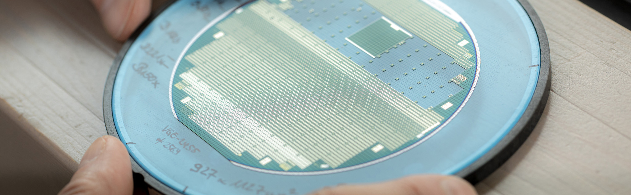
In the business area "III‑V Solar Cells, Modules and Concentrating Photovoltaics", we are working on the most efficient PV technology and looking for economically attractive solutions. The III‑V solar cells we develop are known for their high performance and long-term stability and we continue to set new benchmarks with international record values.

One focus of our research is to reduce the manufacturing costs through new production processes. In addition to requirements from space and concentrator photovoltaics (CPV), we also address solutions for mass markets, such as vehicle-integrated photovoltaics (VIPV) for electromobility.

With the help of our excellent laboratory infrastructure, we work both on the development and optimization of next-generation solar cells and on adapting these devices to the specific requirements of our customers. We cover a wide range of topics, such as ultra-thin flexible cells and modules, engineered substrates with different lattice constants, innovative processes for cost-effective cell production, nanostructured mirrors, and advanced measurement technology. In concentrating photovoltaics, we cover all aspects of solar cells, optics, module technology and systems, up to, for example, the production of solar hydrogen. Finally, we use our expertise in the development of photonic and power electronic components for other applications, such as optical power transmission or thermophotovoltaics (TPV).


Development of III-V Silicon Tandem Solar Cells

III-V/Si tandem solar cell
© Fraunhofer ISE
III-V/Si tandem solar cell on a wafer of 100 mm diameter fabricated at Fraunhofer ISE.

III‑V semiconductors have unique properties that make them ideal for efficiently converting the visible and near-infrared regions of the solar spectrum into electricity. When paired with silicon, these materials enable the creation of highly efficient tandem solar cells, incorporating either two or three subcells. Thanks to the high absorption coefficients of III‑V materials, their layers can remain just a few micrometers thick. Integrating these materials with silicon opens promising pathways toward cost-effective manufacturing techniques.

At Fraunhofer ISE, our research is centered on developing monolithic 2-terminal solar cell concepts, where III‑V layers are either grown directly on silicon or transferred from gallium arsenide (GaAs) substrates through advanced wafer bonding or adhesive technologies. We pursue two main approaches:

1. Direct Epitaxy: III‑V semiconductor layers are deposited directly on silicon using cutting-edge MOVPE reactors from Aixtron (2800G4R with 8x6” configuration and CRIUS CCS with 7x4”). This process begins with growing a GaP nucleation layer on silicon, followed by increasing the lattice constant using ternary GaAsP buffer layers to finally enable absorber layers with bandgaps ranging from 1.4 eV (GaAs) to 1.9 eV (GaInP). Recent advancements in growth optimization have reduced defect densities in GaAs-on-silicon layers to below 10⁷ cm⁻². Additionally, we are working on developing advanced absorber layers, barriers, and tunnel diodes.

2. Wafer Bonding/Adhesive Transfer: III‑V layers are first grown on GaAs substrates and then transferred onto partially processed silicon subcells. Connections between the layers are established using direct wafer bonding or transparent conductive adhesives. The resulting structures form monolithic 2-terminal devices. This approach requires cost-effective processes for III‑V layer growth, thin-layer transfer, and GaAs substrate recycling.

Our R&D Services on the Topic Include:

  • Direct epitaxy of III‑V semiconductors on silicon wafers up to 300 mm in diameter (e.g., GaP nucleation, GaPN, GaAsP, GaAs, GaInP).
  • Advanced characterization of defects in III‑V layers (e.g., antiphase domains, stacking faults, lattice mismatch dislocations).
  • Process development and fabrication of III‑V-based devices on silicon.

Our work aims to enable the next generation of high-efficiency, cost-effective solar cells through cutting-edge research and innovation.


Highlights of our Research and Development Activities in III‑V Si Tandem Photovoltaics

III-V Material Development and Epitaxy

CRIUS
© Fraunhofer ISE
CRIUS Close Coupled Showerhead reactor in the MOVPE laboratory of Fraunhofer ISE.

We develop photovoltaic cells based on III‑V semiconductor compounds, which are composed of elements from the third and fifth groups of the periodic table.

For layer production, we have two modern reactors for industrial-scale metal organic vapor phase epitaxy (MOVPE):

  • An AIX2800 G4-TM reactor with an 8x6-inch configuration
  • A CRIUS showerhead reactor for 7x4-inch or 1x300 mm substrates

We Have a Wide Range of Methods Available for Material Characterization:

  • Electrochemical capacitance-voltage (ECV) profiling
  • Spectrally and spatially resolved photoluminescence (PL)
  • Electroluminescence (EL)
  • Cathodoluminescence (CL)
  • X-ray diffraction (XRD)
  • Nomarski differential interference contrast (DIC) microscopy
  • Candela
  • Reflectance anisotropy spectroscopy (RAS)
  • Scanning electron microscopy (SEM)
  • Deep-level transient spectroscopy (DLTS)
  • Electron beam induced current (EBIC) measurements
  • Electron channeling contrast imaging (ECCI)
  • Infrared Fourier spectroscopy
  • Atomic force microscopy (AFM)
  • Hall-Van der Pauw measurements

Our R&D Services in the Topic Include:

  • Monolithic growth of solar cells with up to six sub-cells stacked on top of each other
  • Adaptation to operating conditions (spectrum, intensity, temperature)
  • Development and adaptation of III‑V absorber materials
  • AlGaAs, AlGaInP, GaAsP, GaInAs, GaInAsP, and GaInNAs on GaAs or Ge substrates
  • InGaAs, InGaAsP on InP substrates
  • Development of strain-compensated multi-quantum wells
  • Direct growth of III‑V semiconductors on silicon substrates for the development of III‑V silicon tandem solar cells
  • Development of metamorphic buffer structures and engineered substrates with adapted lattice constants

Process Technology and Device Fabrication

In our cleanroom laboratory, we process epitaxial wafers into functional components. A modern infrastructure is available for this purpose in our Center for High Efficiency Solar Cells. The wafer processing is designed for 8×4-inch or 8×6-inch batches.

The Processes Available and Used in our Laboratories Include:

  • Photolithography for microstructuring
  • Nano-imprint lithography
  • Deposition of metallic and dielectric layers
  • Wet and dry chemical processes
  • Wafer bonding (including GaAs, InP, GaSb, Si, Ge)
  • Chemical mechanical polishing
  • Surface cleaning

Our R&D Services in this Area Include:

  • Implementation of mirror layers
  • Detaching thin epitaxial layers from the substrate (»liftoff«)
  • Fabrication of functional metasurfaces and photonic structures

Modeling and Design of III-V Solar Cells and Devices

We use a variety of different numerical simulation tools to address the complexity of III‑V multi-junction solar cells.

Our Simulation Infrastructure Includes:

  • Transfer matrix solver for optical simulation of multi-layer systems
  • Opto-electrical semiconductor simulation with Sentaurus TCAD for analyzing the generation and recombination of charge carriers, charge carrier transport at heterojunctions, tunneling processes and photon recycling
  • Electrical network model to optimize contact structures (shading, series resistance losses)
  • Detailed-balance calculations of new solar cell concepts, including determining the ideal band gap combination for various numbers of sub-cells, temperatures and reference spectra
  • Calculating the yield of multi-junction solar cells for various locations, taking into account the influence of the material combination on spectral fluctuations over the course of a day and a year

A comprehensive material database is essential for all simulations. This includes a wide range of III‑V compounds, as well as other typical semiconductors, dielectrics and metals.

Characterization of III-V Solar Cells and Modules

Space solar cell during measurement
© Fraunhofer ISE
Space solar cell during measurement of the calibrated current-voltage characteristic with the multi-source solar simulator.

The precise determination of the performance data of photovoltaic components plays an important role in both research and development and in the production of III‑V solar cells and modules. The CalLab PV Cells at Fraunhofer ISE precisely measures all types of solar cells according to international standards.

A wide range of methods are available for characterizing III‑V multi-junction solar cells:

  • Spectral response of multi-junction solar cells with up to six sub-cells
  • Calibrated measurement of current-voltage (I-V) characteristics
    • Multi-source simulators (three- and six-source simulators) for characterization under defined spectral conditions (AM1.5g, AM1.5d, AM0, indoor spectra, etc.)
    • Spectrometric characterization to quantify the behavior under variable spectrum
    • Four-source flash simulator for spectrally adapted characterization of concentrator solar cells (up to 1500-fold concentrated solar radiation)

In addition, we work on the characterization of concentrator modules and systems. Through our participation in IEC TC 82 WG 7, we have helped to shape the development of international standards for concentrator photovoltaics, as well as the determination of the performance of hybrid PV/CPV modules. Our test facility for CPV modules with a tracking unit on the roof of Fraunhofer ISE allows the standardized characterization and power rating of CPV modules. An indoor laboratory measurement set-up also offers the possibility of conducting measurements on concentrator modules in the laboratory. The measurement set-up generates sun-like, parallel light with the help of a parabolic mirror.


Assembly and Packaging Technology, Reliability Tests for III-V Solar Cells and Modules

Climatic chambers for the investigation of reliability
© Fraunhofer ISE
Climatic chambers for the investigation of reliability.

In the premises of Con-TEC (Concentrator Technology Evaluation Center), we develop assembly and connection technologies and production processes for the manufacturing of concentrator modules, densely packed receivers, e.g. for tower power plants or for thermophotovoltaics, as well as packages for laser power cells. In addition to industry-standard equipment, we use inline and offline characterization tools for the quality assurance of assemblies and modules.

Another research topic is the reliability analysis of individual components. To investigate the long-term stability of modules and components, accelerated aging tests are carried out (temperature aging, temperature cycling, damp-heat test, damp-freeze test, UV irradiation).

Our R&D Services in this Area Include:

  • Development of assembly and connection technologies for concentrator photovoltaics
  • Finite element modeling
  • Reliability testing of assemblies
  • Aging tests

Concentrartor Photovoltaic Modules

In concentrating photovoltaics (CPV), sunlight is focused onto small concentrator solar cells using optical systems. Highly efficient III‑V multi-junction solar cells, which were originally developed for use in space, are used here.

A relevant current development in this context is the miniaturization of the components, in particular the concentrator solar cells and, consequently, the optics on a small scale. In analogy to micro-LED developments, this is referred to as micro-CPV technology, usually defined by solar cells with edge lengths of less than one millimeter. The advantage of this technology is that, on the one hand, the solar cells can be mounted directly on conductor tracks without their own substrate (chip-on-board), and, on the other hand, parallelized high-throughput processes can be used for assembly and contacting. This promises an economically attractive cost structure. Fraunhofer ISE combines unique expertise in this field, ranging from semiconductor physics and III-V multi-junction solar cells to module manufacturing technologies and reliability analyses, through to system integration and energy yield modeling.

Our R&D services in this Area Include:

  • Development and optimization of CPV module designs
  • Optical, thermal, and electrical modeling
  • Optical characterization of concentrator optics
  • Electrical characterization of CPV modules in the laboratory and in outdoor test facilities
  • Power rating and analysis of environmental influences
  • Energy yield modeling

Highlights of our R&D Activities

R&D Infrastructure

This infrastructure is available to us at Fraunhofer ISE for our research and development activities:


Center for High Efficiency Solar Cells

We test and optimize advanced PV technologies in more than 1000 m² of state-of-the-art clean room and laboratory space. Innovative processes and technologies are researched in this center for future use in industry, including wet-chemical processes, photo and laser lithography, nanoimprint laboratory, vapor deposition of metals and dielectrics.


CalLab PV Cells

The accredited calibration laboratory CalLab PV Cells at Fraunhofer ISE offers high-precision, reproducible calibrations and measurements of all types of solar cells according to international standards, for example, spectral responsivity/quantum efficiency, reflectance, current-voltage measurements, especially under variable spectra and intensities, various broadband and laser light sources as well as filters are available.


Concentrator Technology Evaluation Center Con-TEC

Con-TEC has a wide range of assembly and connection technologies available for the development and assembly of customized modules and packages. We test components and production processes with a focus on reliability and material analysis. We develop prototypes and produce small series to evaluate new components, designs and processes.

Selected Reserach-Projects


50 Prozent

Monolithic III-V Multi-Junction Solar Cells with More than 50 % Efficiency under Concentrated Irradiation


micro-CPV

Development of a Highly Concentrating CPV Module Based on Modern Micro-Production Technology


H2Demo

Development of Demonstrators for Direct Solar Water Splitting


HIPERION

Hybrid Photovoltaics for Efficiency Record using Integrated Optical Technology


QuintuMod

Development of a Low-cost and High Efficient Solar Module Using a Solar Cell with 5-pn Junctions


HyCon

Solar Hydrogen Generation Using a HyCon System


PoTaSi

Demonstration of the Potential of Monolithic Tandem Solar Cells Made of III-V Semiconductors and Silicon

Current Publications on the Topic "III-V Solar Cells, Modules and Concentrator Photovoltaics"