| Duration: | May 2015 - April 2019 |
| Contracting Authority/ Sponsors: | European Union |
| Project Partners: | Lund Universitet (SE), Sol Voltaics AB (SE), Université Paris-Sud (FR), Universiteit Leiden (NL), IBM Research GmbH (CH), Centre National de la Recherche Scientifique (FR) |
| Website: | https://nano-tandem.ftf.lth.se/ |
| Project Focus: |
Nano-Tandem – Nanowire-based Tandem Solar Cells


Silicon-based photovoltaic cells are the dominating technology for terrestrial solar electricity generation. After decades of R&D, silicon solar cells are now nearing the theoretical limit with efficiencies of over 26 % achieved in the laboratory. Higher efficiencies of up to 38.8 % have been reached to date only by multi-junction solar cells based on III-V semiconductors. These materials are much more expensive than silicon and their use in flat modules is not profitable.
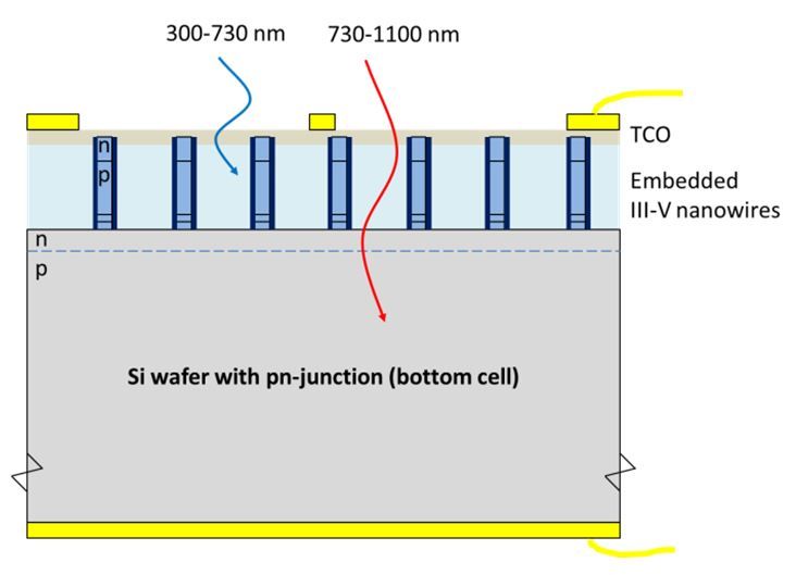
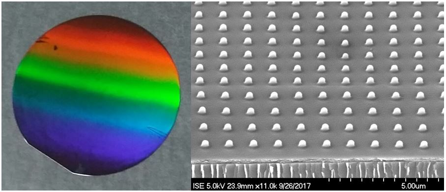
This situation can be improved, however, when the amount of III-V material required is greatly reduced. One way to do this is to grow vertically free-standing nanowires which cover only part of the solar cell area yet still allow for high absorption. Already efficiencies of 13.8 % have been demonstrated for solar cells with InP nanowires. The wires cover only 12 % of the cell surface. The combination of such III-V nanowires with a second silicon solar cell has the potential to simultaneously create powerful devices with efficient use of materials at low costs. In the NanoTandem project our aim is to demonstrate such a tandem solar cell with both a III-V nanowire pn-junction (e.g. GaInP) and a silicon pn-junction. Both of the subcells are connected in series within the cell so that the cell itself has only one front and one rear contact. The manufacture of nanowires on silicon still presents great challenges, which is why we are investigating different processes simultaneously. The wires are grown either directly on the silicon by direct epitaxial growth or rather on a III-V substrate, then embedded in a polymer and transferred to the silicon solar cell. For both of these epitaxial methods, a large-area and scalable pre-structuring of the substrate will be developed by means of nanoimprint lithography. In all, efficiencies of > 25 % shall be demonstrated. The sustainability of this technology is a further theme of the consortium. For this purpose, a life cycle analysis is being carried out in order to prohibit any adverse consequences on the environment and health from the very start.