 Fraunhofer Institute for Solar Energy Systems ISE
News #41
Laser Processing System for Large-Format Wafers Combines High-Throughput and Precision
Every day several million silicon wafers are being produced worldwide for the photovoltaic industry, and the demand is rising sharply. At the same time, the industry is increasingly switching to large wafer formats with an edge length of up to 210 mm. Processing these wafers to produce large-format solar cells with at least the same quality and cycle rate as conventionally sized solar cells presents equipment manufacturers with new challenges, especially for laser processing. To ensure that this processing step does not become a bottleneck in the future, a research team at the Fraunhofer Institute for Solar Energy Systems ISE has developed a novel system concept with industrial partners, which relies on the clever combination of On-the-Fly processing with ultra-fast scanning technology and lasers, high-end optics and sensor technology. Following the successful demonstration of the first system prototype in 2022, which achieved an effective throughput of over 15,000 wafers per hour, a second prototype that uses UV light to create particularly small structures is now in use at Fraunhofer ISE.
"The special design of the demonstrator allows very fine structures to be created on large work pieces at a very high cycle rate," says Dr. Jale Schneider, project manager at Fraunhofer ISE. "A large field of view, rapid processing and fine structures: In laser material processing, the idea is firmly anchored that only two of these three properties are possible to achieve at the same time. With this new system, we were able to fulfill all three requirements simultaneously."
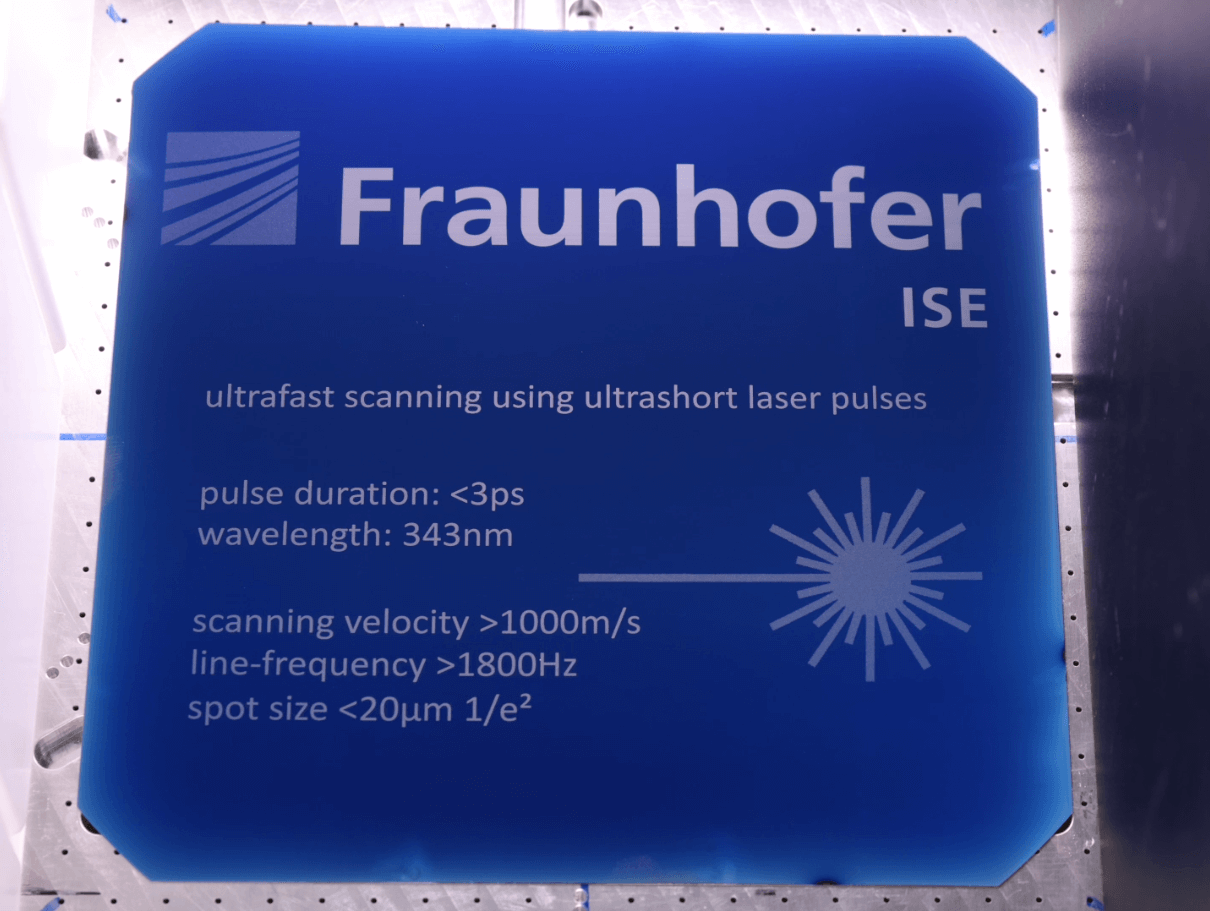
The demonstrator system processes wafer formats up to M12 (210 x 210 millimeters) and creates structures of less than 15 micrometers in size, a reduction of 30 percent compared to the structures realized in current systems based on UV wavelengths. Compared to the more commonly used systems based on IR wavelengths, the size of the created structures are three times smaller. Smallness has advantages. In the case of laser ablated contact openings, for example, the reduced width of the opening leads to narrower conductor paths, which drastically reduce the amount of material required for metallization.
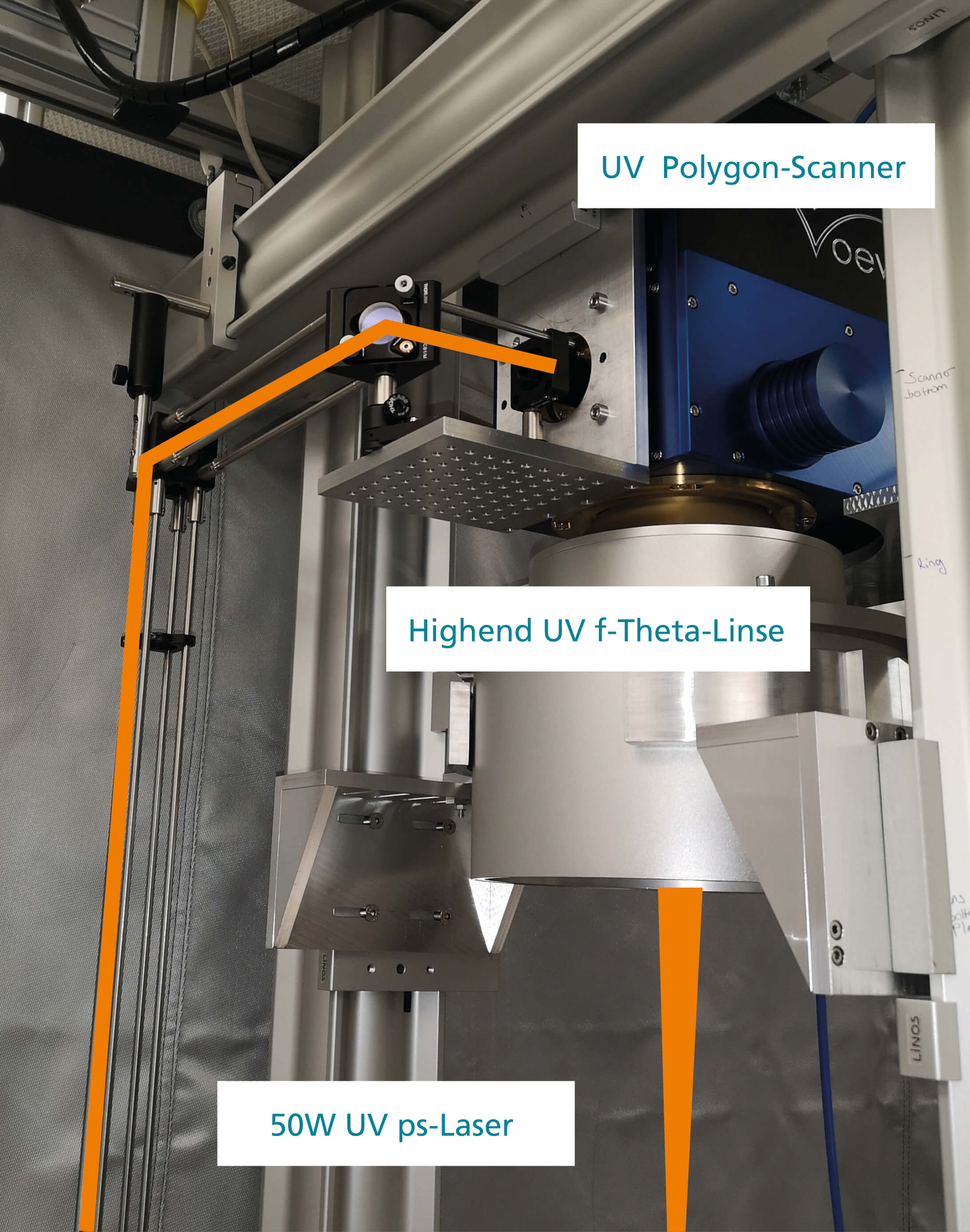
To build the prototype, MOEWE Optical Solutions GmbH constructed an ultra-fast polygon scanner for UV wavelengths with a line frequency of up to 1800 lines per second. "The use of the polygon scanner allows the wafers to be processed 10 to 20 times faster than with conventional galvanometer scanners," says Dr. Florian Rößler from MOEWE Optical Solutions.
EdgeWave GmbH has developed a UV laser that enables a high repetition rate of up to 10 megahertz with a maximum pulse energy of 5.6 microjoules and completely arbitrary pulse sequences. "The realization of a pulse-on-demand function is challenging, but essential for the growing requirements in laser material processing," adds Dr. Keming Du from EdgeWave GmbH. To exploit the potential of the ultra-fast scanner and laser, Fraunhofer ISE integrated them with high-end optics, a linear stage and a beam guidance to create a complete system. The setup is currently being used to test new process regimes and to determine the increase in throughput. Further development topics address synchronization and absolute accuracies of the system components. Both of these aspects play a critical role at such high speeds and small structures.
![Specs Laser Processing System [ PNG 1.28 MB ]](/content/dam/ise/de/images/news/2023/Specs_Laser-Anlage_FraunhoferISE.PNG)
![Layout laser processing system [ JPG 2.64 MB ]](/content/dam/ise/de/images/news/2023/Laser-Anlage-Aufbau_FraunhoferISE.jpg)
The new system concept enables solar cell manufacturers to carry out laser processing at maximum speed without having to compromise on the size of the structure or processing field.
Last modified: