| Duration: | July 2012 - June 2016 |
| Contracting Authority/ Sponsors: | German Federal Ministry of Economic Affairs and Energy (BMWi) |
| Project Partners: | Rauschert Gruppe, Vallis Solaris |
| Project Focus: |
HighVolEpi – High-Throughput Silicon-Based Films and Silicon Epitaxy


Direct deposition of crystalline silicon layers from chlorosilanes is an attractive option for photovoltaics to save large amounts of ultrapure silicon material and energy. Thus, based on long-term experience with CVD processes and systems, Fraunhofer ISE developed and built the “ProConCVD” system for high-throughput coating at atmospheric pressure. The objective of the “HighVolEpi” project is the optimization of Si-based coating processes with respect to layer quality, layer homogeneity and system uptime and to check their usability in photovoltaics. The investigated processes were polycrystalline Si, homoepitaxially grown Si, polycrystalline silicon carbide (SiC) as well as a hydrogen-supported reorganization process for porous Si layer stacks.
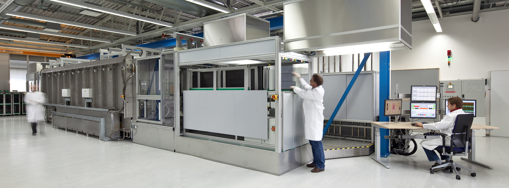
Direct implementation of chlorosilanes in a silicon absorber layer, without the complex and high-loss path via the Siemens process, followed by a crystallization and cutting process, promises great saving in material and energy consumption and enables further cost reductions for photovoltaics modules. We were able to implement the requirement in the photovoltaics industry of high throughput (inline process) with high quality of the deposited layers in a production-relevant system “ProConCVD” (Fig. 1).
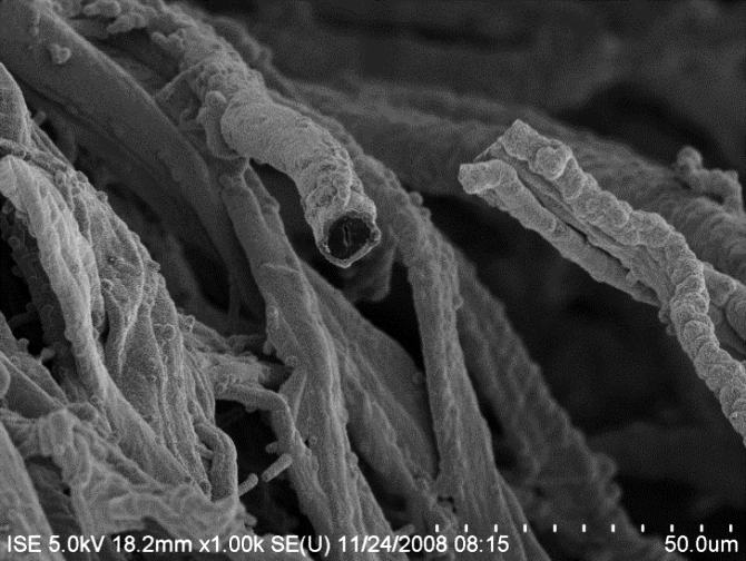
Within the scope of the »HighVolEpi« project, already available processes were optimized, mainly with respect to low metal contamination and surface homogeneity. This was realized using extensive simulations as well as design improvement measures. The optimization measures allowed to transfer the reorganization process from lab scale to an inline system for the first time. The reorganization process is an important step for producing epitaxial wafers (“EpiWafer”) with an area of 156 x 156 mm2. This process reorganizes porous layer stacks so that a separating layer is created allowing lifting the EpiWafer off the substrate. Beyond that, processes for depositing polycrystalline silicon with a thickness of a few µm on oxide surfaces were improved regarding layer thickness homogeneity. For example, coating of graphitic components with an ultrapure polycrystalline SiC layer (Fig. 2) represents another focus in the project. Deposition areas of approx. 500 x 2500 mm2 with fully closed and conformly mapped surfaces represented successful project completion.